팬아웃 패키징 시장 : 시장 점유율 분석, 산업 동향 및 통계, 성장 예측(2025-2030년)
Fan Out Packaging - Market Share Analysis, Industry Trends & Statistics, Growth Forecasts (2025 - 2030)
상품코드:1687980
리서치사:Mordor Intelligence
발행일:2025년 03월
페이지 정보:영문
라이선스 & 가격 (부가세 별도)
ㅁ Add-on 가능: 고객의 요청에 따라 일정한 범위 내에서 Customization이 가능합니다. 자세한 사항은 문의해 주시기 바랍니다.
ㅁ 보고서에 따라 최신 정보로 업데이트하여 보내드립니다. 배송기일은 문의해 주시기 바랍니다.
한글목차
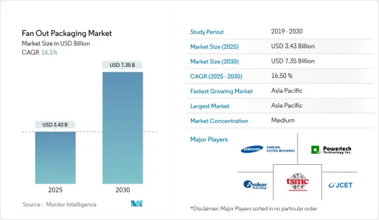
팬아웃 패키징 시장 규모는 2025년에 34억 3,000만 달러로 추정되고, 2030년에는 73억 5,000만 달러에 이를 것으로 예측되며, 시장 예측 기간 2025년부터 2030년까지 CAGR 16.5%로 성장할 전망입니다.
이 시장의 확대는 반도체를 기반으로 한 기술의 진보 및 다양한 분야에서 수요의 급속한 확대가 원동력이 되고 있습니다.
주요 하이라이트
팬아웃 웨이퍼 레벨 패키징(FOWLP)은 고성능으로 에너지 효율이 뛰어난 박형 및 소형 패키지가 요구되기 때문에 스마트폰 등 실장 면적이 중시되는 디바이스에 대한 용도가 확대되고 있습니다. 또한 최근 스마트폰에는 평균 5-7개의 웨이퍼 레벨 패키지(특히 팬아웃)가 탑재되어 있어 그 수는 앞으로도 증가할 것으로 예상되고 있습니다. 이는 기존의 패키지 온 패키지(PoP) 메모리 온 로직 솔루션을 점차적으로 대체하고 있기 때문입니다.
또한 다양한 분야에서 인공지능과 머신러닝 용도가 진행되고 있기 때문에 시장에서의 고성능 컴퓨팅 탑재가 증가하고 있습니다. UHD 팬아웃 기술은 클라우드, 5G, 자율주행차, AI 칩에 대한 용도가 기대되어 예측 기간 중 패키징 동향을 선도합니다.
한국의 반도체 산업은 3D TSV(실리콘 관통 전극), 패키징, FoWLP(팬아웃 웨이퍼 레벨 패키징), FoPLP(팬아웃 패널 레벨 패키징) 기술을 개선하여 반도체의 성능과 집적도를 높이기 위해 보다 효과적으로 노력하고 있습니다.
2021년 12월, 네페슬라우는 Deka의 M 시리즈 팬아웃 기술을 이용한 세계 최초의 600mm×600mm 대형 패널 레벨 패키지(PLP) 생산에 성공했다고 발표했습니다. 이 사업에 따르면 팬아웃 패널 레벨 패키징(FOPLP) 라인은 3분기에 고객 인증을 통과하고 안정적인 수율을 확립하고 본격적인 양산을 시작했습니다.
한국 기업은 기존에 이러한 시스템을 해외기업에 의존하고 있었기 때문에 코스테크는 앞으로 큰 수입 대체 효과를 기대하고 있습니다. 임시 웨이퍼 본더 및 디본딩 기술은 팬아웃 패키징 공정에서 사용할 수 있습니다.
COVID-19의 발생으로 반도체 패키징 시장은 물품의 이동이 제한되어 반도체 공급망에 심각한 혼란이 생겨 성장이 둔화되었습니다. 2020년 1분기 COVID-19는 반도체 공급업체와 유통 채널 고객에게 낮은 재고 수준을 제공했습니다. 코로나 바이러스의 발생으로 시장은 장기적인 영향을 받을 것으로 예상됩니다.
팬아웃 패키징 시장 동향
고밀도 팬아웃이 큰 점유율을 차지
미드레인지에서 하이엔드 용도를 대상으로 하는 고밀도 팬아웃은 1mm2당 6-12개의 I/O를 가지며 라인/스페이스는 15/15μm-5/5μm입니다. 고밀도 팬아웃 패키징은 휴대폰 패키징의 폼 팩터와 성능 요구 사항을 충족시키기 위해 널리 사용되었습니다. 이 기술의 주요 구성 요소는 재분배 층(RDL) 금속과 메가 필러 도금입니다.
TSMC의 InFO 기술은 고밀도 팬아웃의 가장 두드러진 예 중 하나입니다. 이 기술은 애플리케이션 프로세서(AP)와 같은 핀 수가 많은 용도를 대상으로 합니다. 이 회사는 FO-WLP 분야를 inFO-Antenna-in-Package(AiP), inFO-on-Substrate 등의 기술로 확대할 계획입니다. 이러한 패키지는 자동차, 서버, 스마트폰에 사용됩니다. 애플은 이 신기술을 재빨리 채용한 기업의 하나로, 2016년 후반에 발표된 iPhone 7의 A10 애플리케이션 프로세서에 채용되었습니다.
이러한 이점으로부터 2021년 12월, 퀄컴과 미디어 테크 양사는 아이폰 칩의 패키지에 TSMC의 InFO_PoP 기술을 이용하는 애플의 발자취를 따라, 자사의 플래그쉽 스마트폰 애플리케이션 프로세서의 제조에 팬아웃 PoP를 채용하는 것을 검토했습니다.
또한 반도체 시장의 성장과 고밀도 팬아웃 패키징 솔루션의 개발이 예측 기간 동안 시장 성장을 가속할 것으로 예상됩니다. 예를 들어, 2021년 7월 세계 최고의 복합 회로 제조업체이자 기술 솔루션 공급업체인 Changdian Technology는 XDFOI 칩용 초고밀도 팬아웃 패키징 옵션의 전체 라인을 공식적으로 도입했습니다. 이는 칩 이기종 집적을 위한 비용 효율성, 고밀도 연결성, 고집적 및 고신뢰성 솔루션을 제공하는 것을 목표로 합니다.
고밀도 팬아웃 웨이퍼 레벨 패키징(FOWLP)의 제조 방법에서도 첨단 패키징이 이루어지고 있습니다. 신뢰성, 에너지 효율, 디바이스 속도 및 다기능 집적을 향상시키면서 칩 크기 및 높이를 줄이고 제조 비용을 줄이는 솔루션이 개발되었습니다. 예를 들어, SPTS Technologies는 고밀도 팬아웃 웨이퍼 레벨 패키징과 같은 고급 패키징 방식을 위해 주요 반도체 패키징 기업에 여러 플라즈마 에칭 및 증착 공정 기술을 제공합니다.
게다가 고밀도 팬아웃(HDFO) 패키지는 웨이퍼 레벨 프로세싱의 제조 능력과 토르 구리(Cu) 필러나 스루 패키지 비아(TPV) 등의 스루 몰드 상호 접속이나 선진 플립칩 패키징 기술을 사용하여 3D 구조를 만드는 능력에 의해 이러한 소형화의 요구에 대응할 수 있습니다.
시장에서 큰 점유율을 차지하는 대만
대만에는 주요 반도체 제조 기업이 있으며, 특히 PLP와 같은 첨단 패키징 수요를 뒷받침하고 있습니다. 정부의 싱크탱크인 과학기술 국제전략센터에 따르면 대만 생산고는 2021년 25.9% 증가한 1,470억 달러로 성장한 것으로 평가되었습니다.
반도체산업협회(SIA)에 따르면 아시아태평양은 세계 반도체 매출의 50% 이상을 벌어들입니다. 이것은 대만 벤더에게 반도체 용도 증가에 FOWLP를 공급할 기회를 제공하게 됩니다.
대만의 대부분의 기업은 팬아웃 패키지의 생산 능력을 확대하고 있으며, 이는 수출을 증가시키고 국내 시장의 발전에 기여할 것으로 기대됩니다. 예를 들어 최근 주조 산업으로의 복귀를 발표한 인텔은 동시에 뉴멕시코주에 35억 달러를 투자하고 2022년 후반에 운영을 시작하는 반도체 패키지 공장을 건설할 예정입니다.
게다가 2021년 6월에는 순수 반도체 후공정(OAST)의 ASE가 반도체의 수급 부족에 대응하기 위해 선진 패키징 설비에 대한 투자를 시작했습니다. 한미 세미컨덕터로부터 WLP, PLP 공정용 반도체 제조장치를 대량으로 구입하여 확대를 가속화하고 있습니다.
또한 5세대(5G) 무선 통신과 고성능 컴퓨팅 시장 개척이 제조업체의 신기술 개발을 가능하게 하고 있습니다. 예를 들어 TSMC는 고밀도 팬아웃 분야의 유일한 선두 주자로 FO-WLP 분야를 inFO-Antenna-in-Package(AiP) 및 inFO-on-Substrate(oS)와 같은 기술로 확장할 계획입니다.
팬아웃 패키징 업계 개요
시장은 적당히 단편화되고 많은 기업이 존재합니다. 세계의 팬아웃 패키징 시장에서 사업을 전개하고 있는 주요 기업으로는 Taiwan Semiconductor Manufacturing Company Limited, Jiangsu Changjiang Electronics Tech Co., Amkor Technology Inc., Samsung Electro-Mechanics, Powertech Technology Inc. 등이 있습니다. 이 기업들은 시장 점유율을 확대하기 위해 제품 혁신, 합병, 인수 등의 개발에 몰두하고 있습니다.
2021년 11월-반도체 패킹 및 테스트 서비스 공급업체인 Amkor Technology, Inc.는 베트남 박닌에 지능형 공장을 건설하려는 의향을 표명했습니다. 이 공장의 초기 단계는 선진 시스템 인 패키지(SiP)의 조립 및 테스트 서비스를 세계 유수의 반도체 및 전자 기기 제조 기업에 제공하는 것에 집중합니다.
2021년 2월-삼성 주조는 애리조나, 뉴욕, 텍사스 주 당국에 미국에서 최첨단 반도체 제조 시설의 건설을 요구하는 서류를 제출했습니다. 텍사스주 오스틴 근교에 건설 예정인 공장은 총공비 170억 달러 이상, 1,800명의 고용 창출이 전망되고 있습니다. 2023년 4분기까지 가동할 예정입니다.
기타 혜택 :
엑셀 형식 시장 예측(ME) 시트
3개월간의 애널리스트 서포트
목차
제1장 서론
조사 전제조건 및 시장 정의
조사 범위
제2장 조사 방법
제3장 주요 요약
제4장 시장 인사이트
시장 개요
업계의 매력도-Porter's Five Forces 분석
공급기업의 협상력
구매자의 협상력
신규 참가업체의 위협
경쟁 기업간 경쟁 관계
대체품의 위협
시장에 대한 COVID-19의 영향
제5장 시장 역학
시장 성장 촉진요인
고성능 컴퓨팅 및 5G 무선 네트워킹의 보급
시장 성장 억제요인
제조에 따른 제조 비용 과제
FOPLP 시장 기회
시장에 대한 COVID-19의 영향
제6장 시장 세분화
유형별
코어 팬아웃
고밀도 팬아웃
초고밀도 팬아웃
캐리어 유형별
200mm
300mm
패널
비즈니스 모델별
OSAT
파운더리
IDM
지역별
대만
중국
미국
한국
일본
유럽
제7장 팬아웃 패키징 벤더 랭킹 분석
제8장 경쟁 구도
기업 프로파일
Taiwan Semiconductor Manufacturing Company Limited
Jiangsu Changjiang Electronics Tech Co.
Samsung Electro-Mechanics
Powertech Technology Inc.
Amkor Technology Inc.
Advanced Semiconductor Engineering Inc
Nepes Corporation
제9장 투자 분석
제10장 미래의 전망
AJY
영문 목차
영문목차
The Fan Out Packaging Market size is estimated at USD 3.43 billion in 2025, and is expected to reach USD 7.35 billion by 2030, at a CAGR of 16.5% during the forecast period (2025-2030).
The expansion of this market is being driven by technological advancements in semiconductor-based technologies and rapidly expanding demand in various sectors.
Key Highlights
Fan-out wafer level packaging (FOWLP) finds its increased application in footprint-sensitive devices such as smartphones due to the requirement of high-performing, energy-efficient thin- and small-form-factor packages. Further, on average, five to seven wafer-level packages (especially fan-out) can be found in modern smartphones, and the numbers are expected to increase in the future. This is because they are gradually replacing the more traditional package-on-package (PoP) memory-on-logic solutions.
Moreover, the increasing application of artificial intelligence and machine learning in various fields has increased the installation of high-performance computing in the market. UHD fan-out technology is expected to be applied to the cloud, 5G, autonomous cars, and AI chips and will lead the packaging trend during the forecast period.
South Korea's semiconductor industry is continuing to put in efforts to improve and make 3D TSV (Through-silicon via), packaging and FoWLP (Fan-out Wafer-Level Packaging), and FoPLP (Fan-out Panel-Level Packaging) technologies more effective to raise the performance of semiconductors and the degree of integration.
In December 2021, Nepes Laweh corporation announced the successful production of the world's first 600 mm x 600 mm large Panel Level Packaging (PLP) using Deca's M-Series fan-out technologies. The Fan-out-Panel Level Packaging (FOPLP) line passed customer certification in the third quarter, established a consistent yield, and commenced full-scale mass production, according to the business.
Because South Korean companies depended on foreign companies for these systems in the past, KOSTEK is expecting a huge import substitution effect in the future. Its temporary wafer bonder and debonding techniques can be used during a fan-out packaging process.
With the outbreak of COVID-19, the semiconductor packaging market witnessed a decline in growth due to restrictions on the movement of goods and severe disruptions in the semiconductor supply chain. In Q1 2020, COVID-19 caused low inventory levels for clients of semiconductor vendors and distribution channels. The market is expected to witness a long-term impact due to the coronavirus outbreak.
Fan Out Packaging Market Trends
High-Density Fan-Out to Hold a Significant Share
Targeted for mid-range to high-end apps, high-density fan-out has between 6 to 12 I/Os per mm2 and between 15/15 μm to 5/5 μm line/space. High-density fan-out packaging gained popularity to address the form factor and performance requirements for mobile phone packaging. Key building blocks for this technology comprise redistribution layer (RDL) metal and mega pillar plating.
TSMC's InFO technology is one of the most notable examples of high-density fan-out. This technology targets higher pin count applications, such as application processors (AP). The company plans to extend its FO-WLP segment into technologies like inFO-Antenna-in-Package (AiP) and inFO-on-Substrate. These packages are used in automobiles, servers, and smartphones. Apple was one of the early adopters of this new technology, which used it in the A10 application processor of the iPhone 7, introduced in late 2016.
Owing to such benefits, in December 2021, Qualcomm and MediaTek both considered adopting fan-out PoP in the production of their flagship smartphone application processors, following in the footsteps of Apple utilizing TSMC's InFO_PoP technology to package its iPhone chips.
Furthermore, semiconductor market growth along with development in high-density fan-out packaging solutions is expected to propel market growth over the forecast period. For instance, in July 2021, Changdian Technology, the world's premier combined circuit manufacturer and technology solution provider, revealed the official introduction of the entire line of very high-density fan-out packaging options for XDFOI chips, that are intended to deliver cost-effective, high-density connectivity, high-integration, and high-reliability solutions for chip heterogeneous integration.
Advancements are also made in the fabrication method of manufacturing High-Density Fan-Out Wafer Level Packaging (FOWLP). Solutions are being developed to reduce chip size/height and lower production costs while improving reliability, energy efficiency, device speed, and multi-function integration. For instance, SPTS Technologies offers multiple plasma etch and deposition process technologies to leading semiconductor packaging companies for advanced packaging schemes such as that of high-density fan-out wafer-level packaging.
Moreover, high-density fan-out (HDFO) packages can address these needs of miniaturization by fabrication capabilities of wafer-level processing coupled with its ability to create 3D structures using through-mold interconnects such as tall copper (Cu) pillars and through package vias (TPVs) and advanced flip chip packaging technologies.
Taiwan to Hold a Significant Share in the Market
Taiwan houses some of the major semiconductor manufacturing companies which are fueling the demand for advanced semiconductor packaging, especially in PLPs. According to a government think tank, Science and Technology International Strategy Center, Taiwan's output was expected to grow by 25.9% in 2021 to USD 147 billion.
According to the Semiconductor Industry Association (SIA), Asia-Pacific generates more than 50% of revenue for global semiconductor sales; this, in turn, provides Taiwanese vendors with an opportunity to supply FOWLP for increased semiconductor applications.
Most of the companies in the country are expanding their production capacity of Fan-out packaging, which is further expected to increase exports and help develop the local market. For instance, Intel, which recently announced its return to the foundry industry, will simultaneously invest USD 3.5 billion in New Mexico to construct a semiconductor packaging factory that will begin operations in the second half of 2022.
Further, in June 2021, ASE, a pure semiconductor post-processing (OAST), started investing in advanced packaging facilities in response to the supply and demand shortage of semiconductors. It is accelerating the expansion by purchasing a large amount of semiconductor manufacturing equipment for WLP and PLP processes from HANMI Semiconductor.
Also, the growing market for fifth-generation (5G) wireless communication and high-performance computing has enabled manufacturers to develop newer technologies. For instance, as a sole leader in the High-Density Fan-out segment, TSMC is planning to extend its FO-WLP segment into technologies like inFO-Antenna-in-Package (AiP) and inFO-on-Substrate (oS).
Fan Out Packaging Industry Overview
The market is moderately fragmented, with the presence of numerous players. Some of the major players operating in the global fan-out packaging market include Taiwan Semiconductor Manufacturing Company Limited, Jiangsu Changjiang Electronics Tech Co., Amkor Technology Inc., Samsung Electro-Mechanics, and Powertech Technology Inc., among others. These players indulge in product innovation, mergers, and acquisitions, among other developments, in order to increase market share.
November 2021 - Amkor Technology, Inc., a semiconductor packing and test service supplier, stated that it intends to construct an intelligent factory in Bac Ninh, Vietnam. The proposed factory's initial phase will concentrate on offering Advanced System in Package (SiP) assembling and testing services to the world's premier semiconductor and electronics manufacturing businesses.
February 2021 - Samsung Foundry has filed documents with authorities in Arizona, New York, and Texas seeking to build a leading-edge semiconductor manufacturing facility in the USA. The potential fab near Austin, Texas, is expected to cost over USD 17 billion and create 1,800 jobs. It is expected to go online by the fourth quarter of 2023.
Additional Benefits:
The market estimate (ME) sheet in Excel format
3 months of analyst support
TABLE OF CONTENTS
1 INTRODUCTION
1.1 Study Assumptions and Market Definition
1.2 Scope of the Study
2 RESEARCH METHODOLOGY
3 EXECUTIVE SUMMARY
4 MARKET INSIGHTS
4.1 Market Overview
4.2 Industry Attractiveness - Porter's Five Forces Analysis
4.2.1 Bargaining Power of Suppliers
4.2.2 Bargaining Power of Buyers
4.2.3 Threat of New Entrants
4.2.4 Intensity of Competitive Rivalry
4.2.5 Threat of Substitute Products
4.3 Impact of COVID-19 on the Market
5 MARKET DYNAMICS
5.1 Market Drivers
5.1.1 The Proliferation of 5G Wireless Networking Along with High-performance Computing
5.2 Market Restraints
5.2.1 Manufacturing And Cost Challenges Associated with Production
5.3 Market Opportunities for FOPLP
5.4 Impact of COVID-19 on the market
6 MARKET SEGMENTATION
6.1 By Type
6.1.1 Core Fan-Out
6.1.2 High-Density Fan-Out
6.1.3 Ultra High-density Fan Out
6.2 By Carrier Type
6.2.1 200 mm
6.2.2 300 mm
6.2.3 Panel
6.3 By Business Model
6.3.1 OSAT
6.3.2 Foundary
6.3.3 IDM
6.4 Geography
6.4.1 Taiwan
6.4.2 China
6.4.3 United States
6.4.4 South Korea
6.4.5 Japan
6.4.6 Europe
7 FAN-OUT PACKAGING VENDOR RANKING ANALYSIS
8 COMPETITIVE LANDSCAPE
8.1 Company Profiles
8.1.1 Taiwan Semiconductor Manufacturing Company Limited