Applied Materials: Competitive Analysis of Served Markets
상품코드:1473282
리서치사:Information Network
발행일:2026년 02월
페이지 정보:영문
라이선스 & 가격 (부가세 별도)
한글목차
소개
Applied Materials는 경쟁이 치열한 반도체 제조 장비 업계에서 기술 리더십, 전략적 시장 포지셔닝, 최신 반도체 제조 과제에 대한 종합적인 접근 방식에 있어 독보적인 입지를 구축하고 있습니다. 반도체 산업이 노드 미세화 및 디바이스 아키텍처의 복잡성 증가에 따라 Applied Materials의 에칭, 증착, CMP, 계측 및 이온 주입 장비의 혁신은 차세대 전자 장치 구현에 필수적인 역할을 할 것입니다. Applied Materials는 끊임없는 혁신과 전략적 선견지명을 통해 반도체 기술과 제조의 미래를 개척하고, 각 시장에서 경쟁사들과 어깨를 나란히 하며 선도하고 있습니다.
에칭 및 증착 기술
Applied Materials는 반도체 소자 제조의 기반이 되는 에칭 및 증착 공정에 강점을 가지고 있습니다. 이 회사의 에칭 장비는 실리콘 기판의 나노 스케일 특성을 정의하는 데 중요한 플라즈마 공정을 정밀하게 제어합니다.
증착은 화학적 증착(CVD), 물리적 증착(PVD), 원자층 증착(ALD) 솔루션을 제공합니다. 이러한 기술은 반도체 소자의 다양한 박막 층을 형성하는 데 필수적이며, 정확성, 공정 효율성 및 진화하는 산업 요구 사항에 대한 적응성에 중점을 두고 있습니다.
CMP 장비
CMP(화학적 기계적 연마) 장비는 제조 공정 간 웨이퍼 표면의 평탄도를 보장하는 Applied Materials의 주력 분야이며, Applied Materials의 CMP 장비는 제조 워크플로우에 통합되어 처리량을 최적화하고 불량률을 감소시켜 반도체 산업의 목표에 부합합니다. 이는 제조 수율과 비용 효율성을 향상시켜 반도체 업계의 목표에 부합합니다.
측정 및 검사 장비
측정 및 검사 장비는 웨이퍼의 특성에 대한 중요한 데이터를 제공하여 공정 조정 및 결함을 조기에 발견할 수 있도록 돕습니다. 이러한 종류의 장비는 품질 관리에 필수적이며, 장치가 점점 더 복잡해짐에 따라 제조업체는 높은 수준의 제품 수율과 작업 효율을 유지할 수 있습니다.
이온 주입 장비
Applied Materials는 반도체 재료의 도핑에 필수적인 이온 주입 기술도 전문으로 하고 있습니다.
이 회사의 임플란터는 도펀트 종, 에너지, 도즈 양을 정밀하게 제어하여 반도체 디바이스에서 원하는 전기적 특성을 구현하는 데 필수적입니다.
이 보고서에 대하여
본 보고서는 세계 반도체 제조 장비 시장의 Applied Materials 실적 동향을 분석했으며, 전체적인 기술개발, 제조, 공급 동향(2012-2023년), 제품 종류별 시장 규모와 점유율, 주요 경쟁사의 전략, 제품, 실적 등의 정보를 정리하여 전해드립니다.
목차
제1장 소개
제2장 Applied Materials 전략
시장 전략
제조 장비 수요 촉진
국제적인 프레전스
고객 요구를 충족
신CEO의 전략
사업 전략
Silicon Systems Group
Applied Global Services
디스플레이
에너지·환경 솔루션
기술 전략
제품 전략
인수 전략
법적 전략
재무 분석
제3장 시장 예측
시장 성장 촉진요인
반도체 시장
기술 동향
경제 동향
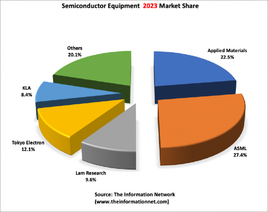
Applied Materials : 세계 시장 리더(2019년까지)
시장 규모와 시장 점유율
화학 증착
물리 증착
드라이 에칭
급속 열처리/산화/확산
실리콘 에피택시
CMP(화학 기계 평탄화)
측정 및 검사
이온 주입
제4장 경쟁 환경
소개
Lam Research
Tokyo Electron Limited
KLA
ASM International
Axcelis
Canon Anelva
Ebara
Eugene Technology
Hitachi High-Technologies
Hitachi Kokusai Electric
Jusung Engineering
KC Tech
Lasertec
Nissin Ion Equipment
NuFlare Technology
Screen Semiconductor Solutions
SEMES
SEN
TES
Ulvac
Wonik IPS
ksm
영문 목차
영문목차
Introduction
In the competitive realm of semiconductor manufacturing equipment, Applied Materials stands
out for its technological leadership, strategic market positioning, and comprehensive approach
to addressing the challenges of modern semiconductor fabrication. As the industry moves
towards smaller nodes and more complex device architectures, Applied Materials' innovations
in etch, deposition, CMP, metrology, and ion implant equipment will continue to play a critical
role in enabling the next generation of electronic devices. Through continuous innovation and
strategic foresight, Applied Materials is not just competing but leading in the markets it serves,
shaping the future of semiconductor technology and manufacturing.
Applied Materials' market leadership is supported by continuous innovation and a strategic
approach to addressing semiconductor manufacturing challenges. The company's investment in
research and development ensures its technologies meet current demands and anticipate
future industry shifts.
As semiconductor fabrication evolves towards more advanced nodes and explores novel
materials and architectures, Applied Materials is poised to play a central role. Its
comprehensive technology portfolio, covering etch, deposition, CMP, metrology/inspection,
and ion implant, positions the company as a key enabler of next-generation semiconductor
devices.
Etch and Deposition Technologies
Applied Materials excels in etch and deposition processes, foundational to semiconductor
device fabrication. The company's etch systems offer precise control over plasma processes,
crucial for defining nanoscale features on silicon substrates. These systems enable the creation
of intricate device structures required for current computing and memory applications.
In deposition, Applied Materials provides solutions across Chemical Vapor Deposition (CVD),
Physical Vapor Deposition (PVD), and Atomic Layer Deposition (ALD). These technologies are
critical for forming the various thin-film layers in semiconductor devices, with a focus on
precision, process efficiency, and adaptability to evolving industry requirements.
CMP Systems
CMP equipment is another area of focus for Applied Materials, ensuring the planarity of wafer
surfaces between fabrication steps. The company's CMP systems integrate with fabrication
workflows, optimizing throughput and reducing defectivity. This contributes to improved
manufacturing yields and cost efficiencies, aligning with the semiconductor industry's goals.
Metrology/Inspection Equipment
Metrology and inspection equipment from Applied Materials provides critical data on wafer
properties, facilitating process adjustments and early defect identification. This category of
equipment is vital for quality control, enabling manufacturers to uphold high standards of
product yield and operational efficiency amid increasing device complexity.
Ion Implant Equipment
Applied Materials also specializes in ion implantation technology, essential for doping
semiconductor materials. The company's implanters deliver high precision in dopant species,
energy, and dose control, critical for achieving desired electrical characteristics in
semiconductor devices.
About This Report
This report addressed the Served Available Markets that Applied Materials competes. Namely:
Chemical Vapor Deposition
Physical Vapor Deposition
Dry Etch
Rapid Thermal Processing/Oxidation/Diffusion
Silicon Epitaxy
Chemical Mechanical Planarization
Metrology and Inspection
Ion Implantation
It presents forecasts for each sector and market shares for each equipment type between 2012
and 2023.
Table of Contents
Chapter 1. Introduction
Chapter 2. Applied's Strategies
2.1. Market Strategies
2.1.1. Driving Demand for Processing Equipment
2.1.2. A Global Presence
2.1.3. Meeting Customer Needs
2.1.4. New CEO's Strategy
2.2. Business Strategies 2.
2.2.1. Silicon Systems Group
2.2.2. Applied Global Services
2.2.3. Display
2.2.4. Energy and Environmental Solutions
2.3. Technology Strategies
2.4. Product Strategies
2.5. Acquisition Strategies
2.6. Legal Strategies
2.7. Financial Analysis
Chapter 3. Market Forecast
3.1. Market Drivers
3.1.1. Semiconductor Market
3.1.2. Technical Trends
3.1.3. Economic Trends
3.2. Applied Materials - Global Market Leader Until 2019