


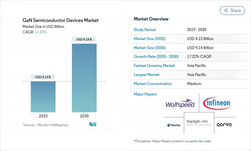
질화갈륨 반도체 장비 시장 규모는 2025년 41억 3,000만 달러로 평가되었고, 2030년에 91억 4,000만 달러로 성장할 전망입니다.

이 급증은 기존 실리콘 대비 GaN이 본질적으로 더 높은 효율, 더 빠른 스위칭, 우수한 열 성능을 제공할 수 있는 능력을 반영합니다. 2024년과 2025년 초 시장 모멘텀은 세 가지 동시 변화에 의해 강화되었습니다. 800V 전기차 파워트레인, 고출력 무선주파수 증폭기가 필요한 대규모 5G 구축, 100W를 초과하는 초소형 USB-C 충전기에 대한 소비자 수요입니다. 동시에 글로벌 에너지 효율 규제가 강화되면서 데이터센터 운영사와 산업용 OEM 업체들이 손실을 줄이고 냉각 비용을 절감하는 GaN 기반 변환 단계로 전환하도록 촉진했습니다. 인피니언, 르네사스 등 기존 기업들이 인수합병을 통해 GaN 생산 능력을 확대하는 한편, 일본과 유럽연합의 지역별 인센티브가 6인치 및 8인치 웨이퍼 생산을 목표로 한 신규 공장 건설을 가속화하며 기업 투자가 이 추세를 뒷받침했습니다.
중국 가전 브랜드들이 초소형 USB PD 충전기로의 급속한 전환을 주도했습니다. 2024년 출시된 모델들은 실리콘 대비 부피를 40% 축소하고 소매 가격을 35% 낮추면서 최대 240W를 제공했습니다. Anker의 GaN Prime 라인은 1.8W/cm³ 이상의 전력 밀도를 달성하여 주머니 사이즈 케이스 내에서 노트북과 휴대폰의 다중 프로토콜 충전을 가능케 했습니다. 원가 절감은 아시아태평양 및 북미 지역에서 주류 채택을 촉진하여, 질화갈륨 반도체 장비 시장 전반에 걸쳐 파급 효과를 일으키는 판매량 증가를 이끌었습니다.
중국, 인도, 일본의 이동통신 사업자들은 2024년에 3.5GHz 이상의 GaN-on-SiC 전력 증폭기를 사용하여 15,000개 이상의 매크로 기지국을 구축했습니다. 이 스위치로 전력 소비를 25% 절감하고 커버리지를 18% 확장하여, 한 주요 일본 통신사의 연간 운영 비용을 1,800만 달러 절감했습니다. 이러한 경제성은 GaN PA 설계 수주를 확고히 하고 질화갈륨 반도체 장비 시장 전반에 걸쳐 잠재적 수익을 확대합니다.
2024년 기준 200mm GaN 에피택셜 웨이퍼를 생산하는 인증 공급업체는 10곳 미만이었습니다. 수율은 실리콘 기준 대비 15-20% 낮아 처리량을 제약하고 프리미엄 가격을 유지시켰습니다. 유럽계 1차 자동차 부품사는 6개월 생산 지연으로 2,800만 유로(3,020만 달러) 상당의 전략적 재고 완충 조치를 취해야 했습니다. 병목 현상은 질화갈륨 반도체 장비 시장의 단기 물량에 부담을 주고 있습니다.
질화갈륨 반도체 장비 시장의 파워 반도체 슬라이스는 2024년 55.2% 점유율을 기록했으며, 2030년까지 연평균 19.1% 성장할 것으로 전망됩니다. 데이터센터 운영사는 98.2% 효율을 달성한 GaN 서버 전원 공급 장비로 업그레이드하여 시설당 230만 달러를 절감했습니다. RF 소자는 5G 대규모 MIMO 인프라 및 방위 레이더의 프리미엄 수요 지속으로 그 뒤를 이었습니다.
성숙기는 전략적 분기점을 알렸다. 인피니언과 같은 실리콘 기존 업체들은 자동차 등급 GaN MOSFET 라인을 확장한 반면, 울프스피드와 같은 RF 전문 기업들은 3.5GHz 이상 매크로 셀을 위한 GaN-on-SiC의 열적 여유 공간을 활용했습니다. 통합 전력 스테이지 공급업체들은 개별 부품 판매를 넘어선 전략으로 더 높은 마진을 확보했습니다. 따라서 질화갈륨 반도체 장비 시장은 통합과 수직적 통합을 동시에 경험하며 규모의 경제 효과를 강화하고 있습니다.
고전자이동도 트랜지스터(HEMT)는 2024년 매출의 57.2%를 차지했으나, 모놀리식 전력 IC는 31.1%의 연평균 복합 성장률(CAGR)로 다른 모든 카테고리를 앞질렀다. 한 중국 스마트폰 OEM은 개별 스위치를 단일 GaN IC로 대체해 충전기 부품 목록(BOM) 비용을 18% 절감했으며, 부품 수를 45% 줄여 양산 확대를 촉진했습니다.
통합은 전자기적 호환성을 개선하고 기생 요소를 줄여주며, 이러한 이점이 질화갈륨 반도체 장비 시장이 시스템 인 패키지(SiP) 설계로 기울어지는 이유를 설명합니다. 모듈 공급업체들은 고전력 설비를 담당하는 반면, 다이오드 판매는 보조 정류 역할에서 꾸준히 유지되고 있습니다.
100-650V 구간은 소비자, 데이터센터, 48V 산업용 레일과 호환되어 2024년 70.3% 점유율을 유지했습니다. 한편 800V 추진 아키텍처의 성장에 힘입어 650V 초과 구간은 연평균 42.2% 성장률로 급성장 중입니다. 한 프리미엄 전기차 브랜드는 900V GaN 스테이지를 활용해 충전 시간을 10-80% 단축한 28분으로 줄였으며, SiC 대비 충전기 무게를 3.2kg 경량화했습니다.
이러한 전환은 새로운 절연 및 테스트 표준을 촉발하며 순수 플레이 공급업체에 도전장을 내밀고 있습니다. 그럼에도 질화갈륨 반도체 장비 시장은 650V 이상의 신뢰성을 검증할 수 있는 기업에게 보상을 제공하며, 수익성 높은 자동차 시장 가치를 열어줍니다.
GaN 반도체 장비 시장은 장비 유형(파워 반도체, 기타), 컴포넌트(트랜지스터, 기타), 정격 전압(100V 미만, 기타), 웨이퍼 사이즈(2인치, 기타), 기판 기술(GaN-On-SiC, 기타), 패키징(표면 실장, 기타), 최종 사용자 산업(자동차, 이동성, 기타), 지역(북미, 남미, 유럽, 아시아)
아시아태평양은 2024년 매출의 38.2%를 차지했으며 CAGR은 29.1%에서 가장 빠른 성장세를 보였습니다. 중국의 갈륨에 대한 접근과 국가 보조금을 통해 이노사이언스사는 세계 최대의 8인치 GaN-on-Si 공장을 동업 타사보다 35% 낮은 비용으로 조업할 수 있었습니다. 한국의 가전 대기업과 일본의 자동차 대기업은 대량 생산의 앵커 고객이 되어 수요와 생산 능력 확대의 선순환을 유지했습니다.
북미는 기술 혁신의 온상이었음. 연방 정부의 CHIPS 보조금 3,500만 달러는 GlobalFoundries가 버몬트 주에서 GaN의 생산 능력을 확대하는 데 도움이 되었습니다. 국방 계약자는 GaN 기반 위상 어레이 레이더를 도입하여 검출 범위를 42% 확대하는 한편, 소비 전력을 18% 삭감하고, 질화갈륨 반도체 장비 시장으로 흐르는 미션 크리티컬한 이익을 나타냈습니다.
유럽에서는 프리미엄 자동차와 산업용 이용 사례가 우선되었습니다. Cambridge GaN Devices는 사업 확장을 위해 3,050만 유로(3,310만 달러)를 조달했는데, 이는 유럽의 고출력 틈새 시장에 대한 투자자의 전망을 반영한 것입니다. 독일의 주요 OEM은 97.8%의 충전기 효율과 30%의 부품 절감을 실현하여 EU의 환경 설계 지령에 적합했습니다. 라틴아메리카, 중동 및 아프리카는 현재 겸손한 점유율이지만 에너지 가격과 인프라 정비가 수렴함에 따라 통신 및 스마트 시티 프로젝트에서 유망한 섭취를 입증하고 있습니다.
The gallium nitride semiconductor devices market size stood at USD 4.13 billion in 2025 and is forecast to touch USD 9.14 billion by 2030, reflecting a robust 17.22% CAGR.
The surge mirrors GaN's intrinsic ability to deliver higher efficiency, faster switching, and superior thermal performance when compared with legacy silicon. Market momentum was reinforced in 2024 and early 2025 by three concurrent shifts: 800 V electric-vehicle powertrains, large-scale 5G rollouts that require high-power radio-frequency amplifiers, and consumer demand for ultra-compact USB-C chargers exceeding 100 W. At the same time, global energy-efficiency regulations tightened, pushing data-center operators and industrial OEMs toward GaN-based conversion stages that cut losses and shrink cooling overhead. Corporate investment underscored the trend as Infineon, Renesas, and other incumbents expanded GaN capacity through acquisitions, while regional incentives in Japan and the European Union accelerated green-field fabs geared to 6-inch and 8-inch wafers.
Chinese consumer-electronics brands propelled a rapid shift toward ultra-compact universal serial bus power-delivery chargers. Models released in 2024 delivered up to 240 W while shrinking volume by 40% relative to silicon equivalents and lowering retail prices by 35%. Anker's GaN Prime line exceeded 1.8 W/cm3 power density, enabling multiprotocol charging for laptops and phones within pocket-sized enclosures. Cost-downs stimulated mainstream uptake across Asia-Pacific and North America, lifting unit volumes that ripple across the gallium nitride semiconductor devices market.
Mobile network operators in China, India, and Japan deployed more than 15,000 macro base stations in 2024 using GaN-on-SiC power amplifiers above 3.5 GHz. The switch trimmed power consumption by 25% and stretched coverage by 18%, translating into USD 18 million annual operating expense savings for one leading Japanese carrier. Such economics cement GaN PA design wins and expand addressable revenue across the gallium nitride semiconductor devices market.
Fewer than 10 qualified suppliers produced 200 mm GaN epitaxial wafers in 2024. Yields sat 15-20% below silicon benchmarks, constraining throughput and sustaining premium pricing. A European Tier-1 automotive supplier recorded a six-month production delay that forced strategic inventory buffers worth EUR 28 million (USD 30.2 million). Bottlenecks weigh on near-term volumes within the gallium nitride semiconductor devices market.
Other drivers and restraints analyzed in the detailed report include:
For complete list of drivers and restraints, kindly check the Table Of Contents.
The power-semiconductor slice of the gallium nitride semiconductor devices market held 55.2% share in 2024 and is projected to compound at 19.1% to 2030. Data-center operators saved USD 2.3 million per facility by upgrading to GaN server power supplies that reached 98.2% efficiency. RF devices followed as 5G massive-MIMO infrastructure and defense radar sustained premium demand.
Maturity signaled a strategic fork. Silicon incumbents such as Infineon expanded automotive-grade GaN MOSFET lines, while RF specialists like Wolfspeed leveraged GaN-on-SiC thermal headroom for >3.5 GHz macro cells. Integrated power-stage providers captured a higher margin by moving beyond discrete sales. The gallium nitride semiconductor devices market, therefore, experiences both consolidation and vertical integration, reinforcing scale advantages.
High-electron-mobility transistors occupied 57.2% revenue in 2024, yet monolithic power ICs outpaced all other categories at 31.1% CAGR. A Chinese smartphone OEM cut the charger bill-of-materials by 18% by replacing discrete switches with a single GaN IC, shrinking part count by 45% and catalyzing volume ramps.
Integration improves electromagnetic compatibility and trims parasitics, benefits that explain why the gallium nitride semiconductor devices market is tilting toward system-in-package designs. Module suppliers address high-power installations, while diode sales remain steady in auxiliary rectification roles.
The 100-650 V corridor kept a 70.3% share in 2024 as it aligns with consumer, data-center, and 48 V industrial rails. Meanwhile, the >650 V band races ahead at 42.2% CAGR, fueled by 800 V propulsion architectures. One premium EV brand slashed 10-80% charge time to 28 minutes using 900 V GaN stages and cut charger mass by 3.2 kg versus SiC.
This transition prompts new isolation and test standards, challenging pure-play suppliers. Nevertheless, the gallium nitride semiconductor devices market rewards those able to validate reliability beyond 650 V, unlocking lucrative automotive value pools.
The GaN Semiconductor Devices Market is Segmented by Device Type (Power Semiconductors, and More), Component (Transistors, and More), Voltage Rating (< 100 V, and More), Wafer Size (2-Inch, and More), Substrate Technology (GaN-On-SiC, and More), Packaging (Surface-Mount, and More), End-User Industry (Automotive and Mobility, and More), and Geography (North America, South America, Europe, Asia-Pacific, and Middle East and Africa).
Asia-Pacific commanded 38.2% of 2024 sales and remained the fastest riser at 29.1% CAGR. China's access to gallium, plus state subsidies, allowed Innoscience to operate the world's largest 8-inch GaN-on-Si plant at costs 35% below peers. South Korea's consumer-electronics titans and Japan's automotive majors seeded high-volume anchor customers, sustaining a virtuous cycle of demand and capacity growth.
North America stayed an innovation hotbed. Federal CHIPS grants of USD 35 million helped GlobalFoundries broaden GaN capacity in Vermont. Defense contractors deployed GaN-based phased-array radars that boosted detection range by 42% while trimming power by 18%, showcasing mission-critical gains that flow into the gallium nitride semiconductor devices market.
Europe prioritized premium automotive and industrial use cases. Cambridge GaN Devices raised EUR 30.5 million (USD 33.1 million) for expansion, reflecting investor belief in high-power European niches. A leading German OEM realized 97.8% charger efficiency and 30% component reduction, aligning with EU eco-design directives. Latin America, the Middle East, and Africa presently hold modest shares yet demonstrate promising uptake in telecom and smart-city projects as energy prices and infrastructure buildouts converge.