


반도체 패키지의 미래를 좌우하는 최첨단 본딩 기술 관련 세계 IP 경쟁 시장에서 주요 기업과 신규 진출기업은 어디일까?
하이브리드 본딩은 유전체 대 유전체 접합과 금속 대 금속 접합을 결합하여 솔더나 기타 접착제를 사용하지 않고 웨이퍼와 웨이퍼, 다이와 웨이퍼, 다이와 다이를 상호 연결합니다. 이 접합 기술은 여러 칩의 수직 적층에 사용되며, 하나의 패키지 내에서 다양한 기능(로직, 메모리, 아날로그, 센서 등)을 가진 다양한 유형의 칩의 3차원 이종 집적 및 상호 운용성을 가능하게 합니다. 하이브리드 접합은 미세 피치(10마이크로미터 이하 또는 1마이크로미터 이하)를 가능하게 하여 상호 연결 밀도와 디바이스 성능에 큰 이점을 제공합니다. 금속과 금속이 직접 접촉하므로 효율적인 열 방출이 촉진되고 기생 지연이 감소합니다. 유전체가 각 금속 패드를 절연하므로 패드 간 신호 간섭이 없습니다.
하이브리드 접합 기술은 2005년 Ziptronix의 DBI-R(direct bond interconnect) 기술 도입으로 등장했으며, 2015년 Tessera(현 Adeia)가 Ziptronix를 인수한 후 2016년에 DBI-R 기술은 삼성 휴대폰 갤럭시 S7에 채택된 소니의 CMOS 이미지 센서(CIS)를 통해 시장에 진입했습니다. 이후 하이브리드 접합 기술은 메모리, 로직, RF, 포토닉스 등 다양한 분야에서 활용되고 있으며, 현재 반도체 산업 전반에 걸쳐 더 많은 기업이 채택하고 있습니다.
지난 5년 동안 하이브리드 접합 기술은 첨단 반도체 패키징의 중요한 원동력이 되었고, 특허 활동이 활발해지면서 경쟁 지적재산권(IP) 환경도 크게 변화했습니다. 주요 특허권자들은 미국, 중국, 유럽에서 지적재산권 지위를 강화하는 한편, 다양한 신규 기업이 특허 환경에 진입하고 있습니다. 현재 반도체 패키징 업계에서 사업을 운영하는 기업은 하이브리드 본딩 기술을 지적재산권 관점에서 면밀히 검토하는 것이 매우 중요합니다.
이러한 배경에서 Knowmade는 하이브리드 접합 공정과 하이브리드 접합 인터커넥트를 사용하는 반도체 소자에 초점을 맞춘 새로운 특허 동향을 분석했으며, 1,600개 이상의 특허 패밀리(발명)에서 5,800개 이상의 특허를 추출했습니다. 추출되었습니다. 이 보고서의 목적은 현재 IP 활동, 주요 IP 기업의 위치, 그들이 특허를 통해 목표로 삼고 있는 활용 분야, 그리고 그들의 특허 포트폴리오가 시장 전략을 어떻게 지원할 수 있는지에 대한 인사이트을 제공하는 것입니다.

특허 분석을 통해 지적재산권(IP) 기업의 위치를 설명하고, IP 포트폴리오를 강화하는 전략을 밝히고, 다른 회사의 특허 활동과 영업의 자유를 제한하는 능력을 강조하고, 유망한 신규 기업을 식별하고, 미래의 지적재산권 리더를 예측할 수 있습니다. 시장에 진입하고 사업을 운영하는 전략을 가진 기업의 비전을 반영해야 합니다. 이 보고서는 하이브리드 접합 기술과 관련된 최신 기술 개발 및 경쟁 IP 환경과 최신 기술 개발에 대한 종합적인 개요를 제공합니다. 이 보고서는 특허 출원, 특허 양수인, 출원 국가, 특허 기술, 대상 용도 등 지식재산의 역동성과 주요 동향을 종합적으로 다루고 있습니다. 또한 지적재산권 리더와 가장 활발한 특허 출원인을 식별하고, 이 분야에서 아직 알려지지 않은 기업 및 신규 진출기업도 조명합니다.
특허는 청구된 발명의 유형(하이브리드 접합 제조 방법 및 인터페이스 엔지니어링, 하이브리드 접합 기술용 장비, 하이브리드 접합 반도체 구조/장비) 및 특허에서 언급된 용도(이미지 센서, 2.5D/3D IC, 3D 적층 메모리, 포토닉스, MEMS, RF, RF 등)에 따라 분류된다, RF 등)에 따라 분류되어 있습니다. 현재 2.5D/3D IC 분야가 특허 활동을 주도하고 있지만, 포토닉스, 마이크로 LED, MEMS, RF 등 기타 활동과 관련된 특허가 급증하고 있습니다.

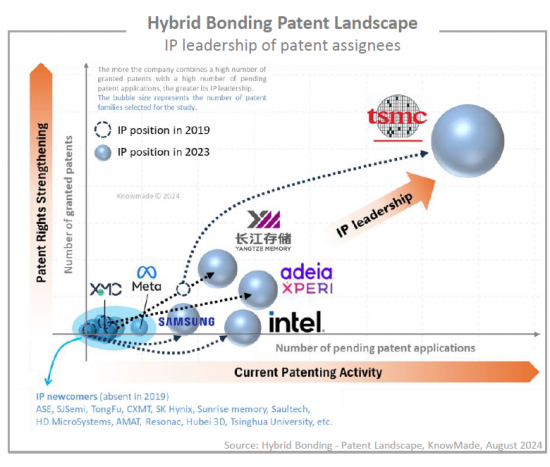
TSMC, Adeia, YMTC, Intel, Samsung은 특허 상황을 주도하고 특허 활동을 활성화하고 주요 국가에서 발명품 보호를 확대하고 있으며, DBI-R 기술의 선구자이자 소유자인 Adeia는 특허를 주장하고 Sony, YMTC, Micron, Kioxia를 포함한 다양한 반도체 기업에 하이브리드 접합 IP 포트폴리오를 라이선싱하는 적극적인 전략을 채택하고 있습니다. 회사의 강력한 IP 포지션에도 불구하고, 다른 기업은 독자적인 하이브리드 접합 특허 포트폴리오를 개발하고 있습니다. 최근에는 더 많은 메모리 제조업체들이 IP 환경에 참여하고 있으며(CXMT, SK하이닉스, Sunrise Memory), OSAT 및 장비/재료 공급업체들이 IP 분야에 진출하고 있다(ASE, TongFu, SJSemi, Applied Materials, Saultech, HD MicroSystems). 이 보고서에서는 주요 기업이 보유한 IP 포트폴리오에 대한 개요를 제공하고, 주요 특허와 최근 IP 활동에 대해 설명합니다. 또한 주요 IP 협업(공동 소유 특허, IP 이전, 라이선스 계약) 및 특허 소송에 대해서도 다루고 있습니다.
이 보고서에는 특허 정보(번호, 날짜, 양수인, 제목, 요약 등), 업데이트된 온라인 데이터베이스에 대한 하이퍼링크(원문, 법적 지위 등), 소속 부문(제조 방법, 장비, 반도체 소자, 이미지 센서, 2.5D/3D IC, 3D 적층 메모리 등) 및 주요 특허가 포함된 광범위한 엑셀 데이터베이스가 포함되어 있습니다.) 및 주요 특허를 포함하여 이 보고서에서 분석된 모든 특허를 포함하는 광범위한 엑셀 데이터베이스가 포함되어 있습니다. 또한 엑셀 파일에는 특허 패밀리 수, 특허 활동 타임라인, 부여된 특허 및 출원 중인 특허 수, 특허 포트폴리오의 지역별 분석 등 통계 분석을 통해 얻은 양수인별 완전한 데이터가 포함되어 있습니다.
TSMC, YMTC, Xperi/Adeia, Intel, Samsung, XMC, Micron, Tongfu Microelectronics, ASE, Meta(Facebook), Nanya Technology, CXMT, Huawei, Onsemi, OmniVision, AMD, ICLeague Technology, Monolithic 3D, UMC/Wavetek, Qualcomm, SJSemi, Saultech, SK Hynix, Tsinghua University, CEA, imec, Galaxycore Microelectronics, Apple, EVG, HD MicroSystems, NCAP, STMicroelectronics, Applied Materials, Resonac, GlobalFoundries, SunRise Memory, Alibaba Group, AP Memory, SMIC, Powerchip Semiconductor Manufacturing, MICLEDI, AMS-Osram, SmartSens Technology, Shenzhen Aoshiwei Technology, MediaTek, IBM, RTX Corporation, pSemi, Winbond electronics, Sony, NVIDIA, Haiguang Information Technology, Shanghai Huali Integrated Circuit Manufacturing, JCET Group, SEMES, Tectus Group, Hanmi, Western Digital, Shibaura Mechatronics, Ningbo Semiconductor International Corporation(NSI), HIDM - Huaian Imaging Device Manufacturer, Bruker, Suzhou Ultiview Technology, KLA, Shanghai Fudan Microelectronics Group, Anhui Xinbiyou Information Technology, Tokyo Electron, Shanghai Yibu Semiconductor, HTSI, GROQ, Dixtech innovation, Qingdao New Core Technology, PsiQuantum, Canon, Infineon, Shanghai Biren Intelligent Technology, Yangtze River Advanced Storage Industry Innovation Center, G-ray Switzerland, 등
Who are the key players and newcomers in the global IP race for the most advanced bonding technology shaping the future of semiconductor packaging?
Hybrid bonding combines dielectric-to-dielectric and metal-to-metal bonds to interconnect wafer-to-wafer, die-to-wafer, or die-to-die without the need for solder or other adhesives. This bonding technology is used for the vertical stacking of multiple chips, enabling 3D heterogeneous integration and interoperability of different types of chips with various functions (e.g., logic, memory, analog, sensors) within a single package. Hybrid bonding enables finer pitch (<10 micrometerm, or even <1 micrometerm) with significant benefits for interconnect density and device performance. The direct metal-to-metal contact facilitates efficient heat dissipation and reduces the parasitic delay. The dielectric insulates each metal pad so that there is no signal interference between the pads.
Hybrid bonding technology emerged in 2005 with the introduction of Ziptronix's direct bond interconnect (DBI-R) technology. In 2015, Tessera (now Adeia) acquired Ziptronix, and DBI-R technology entered the market in 2016 through Sony's CMOS image sensor (CIS) used in Samsung's Galaxy S7 mobile phone. Since then, hybrid bonding technology has been explored for various applications, including memory, logic, RF, and photonics, and it is now being adopted by more companies across the semiconductor industry.
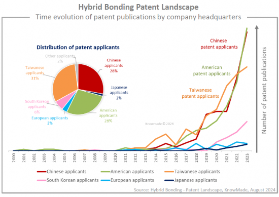
Over the past five years, hybrid bonding technology has become a key enabler of advanced semiconductor packaging, leading to a strong increase in patenting activity and a significant evolution of the competitive intellectual property (IP) landscape. Major patent owners have strengthened their IP positions in the US, China, and Europe, while various new players have entered the patent landscape. It is now crucial for companies operating in the semiconductor packaging industry to closely examine hybrid bonding technology from an IP perspective.
In this context, Knowmade is releasing a new patent landscape report focusing on the hybrid bonding process and semiconductor devices made using hybrid bonding interconnects. Over 5,800 patents from more than 1,600 patent families (inventions) have been selected. This report aims to provide insights into current IP activities, the positions of key IP players, the applications they target in their patents, and how their patent portfolios can support their market strategies.
Through patent analysis, we describe the position of IP players, unveil their strategies to strengthen their IP portfolio, highlight their capability to limit the patenting activity and freedom-to-operate of other firms, identify promising new players, and forecast what would be the future IP leaders. IP competition analysis should reflect the vision of players with a strategy to enter and develop their business in the advanced semiconductor packaging market. In this report, we provide a comprehensive overview of the competitive IP landscape and latest technological developments related to hybrid bonding technology. The report covers IP dynamics and key trends in terms of patents applications, patent assignees, filing countries, patented technologies, and targeted applications. It also identifies the IP leaders, most active patent applicants, and sheds light on under-the-radar companies and new players in this field.
The patents have been categorized according to the type of claimed invention (hybrid bonding manufacturing methods and interface engineering, equipment for hybrid bonding technology, hybrid bonded semiconductor structures or devices) and the applications mentioned in the patents (image sensors, 2.5D/3D ICs, 3D-stacked memories, photonics, MEMS, RF, etc.). The 2.5D/3D IC segment is currently driving patenting activity, while patents related to other applications, such as photonics, microLED, MEMS, and RF, have surged.
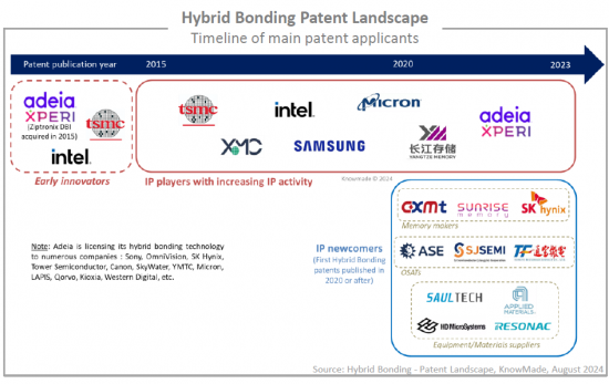
TSMC, Adeia, YMTC, Intel, and Samsung are leading the patent landscape, increasing patenting activity, and expanding invention protection in key countries. As pioneer and owner of DBI-R technology, Adeia has adopted an aggressive strategy to assert its patents and license its hybrid bonding IP portfolio to various semiconductor companies, including Sony, YMTC, Micron, and Kioxia. Despite its strong IP position, other players have been developing their own hybrid bonding patent portfolios. In recent years, more memory makers have become involved in the IP landscape (CXMT, SK Hynix, Sunrise Memory), and OSATs and equipment/materials suppliers have entered the IP arena (ASE, TongFu, SJSemi, Applied Materials, Saultech, HD MicroSystems). In this report, we provide an overview of the IP portfolios held by key players and describe key patents and recent IP activities. Additionally, we highlight the main IP collaborations (co-owned patents, IP transfers, licensing agreements) and patent litigations.

This report includes an extensive Excel database with all patents analyzed in this study, including patent information (numbers, dates, assignees, title, abstract, etc.) and hyperlinks to an updated online database (original documents, legal status, etc.), affiliation segments (manufacturing methods, equipment, semiconductor devices, image sensors, 2.5D/3D IC, 3D-stacked memory, etc.), and key patents. Additionally, the Excel file comprises the complete data by assignee from the statistical analyses, including the number of patent families, timeline of patenting activity, number of granted patents and pending patent applications, and geographical coverage of patent portfolio.
TSMC, YMTC, Xperi/Adeia, Intel, Samsung, XMC, Micron, Tongfu Microelectronics, ASE, Meta (Facebook), Nanya Technology, CXMT, Huawei, Onsemi, OmniVision, AMD, ICLeague Technology, Monolithic 3D, UMC/Wavetek, Qualcomm, SJSemi, Saultech, SK Hynix, Tsinghua University, CEA, imec, Galaxycore Microelectronics, Apple, EVG, HD MicroSystems, NCAP, STMicroelectronics, Applied Materials, Resonac, GlobalFoundries, SunRise Memory, Alibaba Group, AP Memory, SMIC, Powerchip Semiconductor Manufacturing, MICLEDI, AMS-Osram, SmartSens Technology, Shenzhen Aoshiwei Technology, MediaTek, IBM, RTX Corporation, pSemi, Winbond electronics, Sony, NVIDIA, Haiguang Information Technology, Shanghai Huali Integrated Circuit Manufacturing, JCET Group, SEMES, Tectus Group, Hanmi, Western Digital, Shibaura Mechatronics, Ningbo Semiconductor International Corporation (NSI), HIDM - Huaian Imaging Device Manufacturer, Bruker, Suzhou Ultiview Technology, KLA, Shanghai Fudan Microelectronics Group, Anhui Xinbiyou Information Technology, Tokyo Electron, Shanghai Yibu Semiconductor, HTSI, GROQ, Dixtech innovation, Qingdao New Core Technology, PsiQuantum, Canon, Infineon, Shanghai Biren Intelligent Technology, Yangtze River Advanced Storage Industry Innovation Center, G-ray Switzerland, and more.