


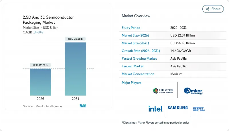
2.5D 및 3D 반도체 패키징 시장은 2025년 111억 2,000만 달러에서 2026년에는 127억 4,000만 달러에 이를 것으로 예측됩니다. 2026-2031년에 걸쳐 CAGR 14.6%로 성장하여 2031년까지 251억 8,000달러에 달할 전망입니다.
초당 테라바이트급 대역폭을 요구하는 AI 훈련 클러스터, 자동차 센서 융합 플랫폼, 공간 제약이 있는 모바일 기기에 힘입어 생태계는 인터포저 용량, 칩릿 표준, 열 효율성 높은 기판에 투자하며 발맞추고 있습니다. 파운드리 업체들은 마진 확보와 로드맵 통제를 위해 패키징을 사내로 이전했으며, OSAT 업체들은 자동차 및 광학 부문를 위한 특수 조립에 집중하고 있습니다. 미국, 유럽, 아시아의 정부 보조금은 지역별 다각화를 지원하지만, 실리콘 인터포저 부족과 냉각 한계로 단기 상승 여력은 제한됩니다. 글래스 코어 기판, 하이브리드 본딩, 공동 패키징 광학 기술이 대중화되면서, 트랜지스터 밀도가 아닌 패키징 혁신이 향후 10년간 시스템 성능을 결정할 것입니다.
현재 1조 개 이상의 매개변수를 초과하는 하이퍼스케일 훈련 모델은 기존 DDR 인터페이스를 포화시켜 GPU 벤더들이 소켓당 3TB/s 대역폭을 제공하는 HBM3 스택과 로직을 공동 패키징하도록 촉진하고 있습니다. 실리콘 관통 전극(TSV)은 트레이스 길이를 단축하고 지연 시간을 줄여, 분리형 레이아웃 대비 시스템 전력 예산을 15% 절감하는 근접 메모리 컴퓨팅을 가능하게 합니다. CoWoS 및 Foveros 플랫폼은 메모리와 가속기 다이를 공유 인터포저에 배치하며, 이 토폴로지는 폼 팩터로 인해 개별 DIMM 사용이 불가능한 엣지 추론 장치에도 이점을 제공합니다. 삼성과 SK하이닉스의 메모리 내 처리 프로토타입은 로직과 스토리지의 경계를 더욱 모호하게 하여, 성능 병목 현상 해소자로서 2.5D 및 3D 반도체 패키징 시장의 위상을 강화하고 있습니다. 데이터센터 운영사들은 이제 랙 에너지 효율 지표를 패키지 메모리 대역폭과 직접 연계하여, 패키징 결정이 하이퍼스케일 확장을 위한 자본 지출 레버로 전환되도록 합니다.
프리미엄 스마트폰은 시스템인패키지(SiP) 모듈 내부에 50개 이상의 기능을 통합하여, 팬아웃 웨이퍼 레벨 패키징을 통해 기판 면적을 40% 축소하고 z-높이를 0.5mm 미만으로 줄입니다. 스마트워치는 밀도를 더욱 높여 100mm² 미만 패키지에 무선 통신, 센서, 전력 관리의 이종 통합을 요구합니다. 차세대 웨어러블용 신축성 전자기기는 유기 기판이 충족할 수 없는 기계적 변형 제약을 추가하여 뒤틀림 방지 RDL-퍼스트 팬아웃 공정 채택을 촉진합니다. 히어러블 및 의료용 웨어러블 기기 확산으로 생체 적합성 캡슐화제와 습기 차단 장치가 필수화되며, 소비자 헬스케어 부문 내 2.5D 및 3D 반도체 패키징 시장 점유율이 확대됩니다. 한때 선택 사항이었던 패키지 레벨 EMI 차폐는 이제 주머니 크기 기기 내 밀리미터파 연결 및 초광대역 거리 측정 기술의 기본 요건이 되었습니다.
개별 CoWoS 라인은 표준 조립 설비 대비 3-4배의 비용이 소요되며, 사이트당 총 투자액을 100억 달러 수준으로 끌어올립니다. 감가상각 기간이 10년으로 연장되면서 OSAT 업체들은 가격 유연성을 저해하는 높은 고정 비용에 묶이게 됩니다. 장비 공급업체의 과점 구조로 인해 장비 납기 기간이 18개월 이상으로 길어지면서 공급망 리스크가 가중됩니다. 소규모 조립업체들은 TSV 식각 모듈이나 하이브리드 본딩 얼라이너를 조달할 수 없어 고급 2.5D 및 3D 반도체 패키징 시장에서 퇴출되며, 이는 파운드리 업체들의 상류 공정 집중화를 초래합니다.
3D TSV 솔루션은 2025년 매출의 43.72%를 차지했으며, 14.85%의 연평균 성장률(CAGR)로 2.5D 및 3D 반도체 패키징 시장 점유율 경쟁에서 선두를 유지하고 있습니다. 삼성의 HBM3E 스택은 평면 레이아웃 대비 장치당 1.15TB/s 대역폭을 제공하며, 풋프린트를 60% 축소하고 기판 전원 레일을 30% 절감합니다.
AI 처리 능력에 대한 수요가 높아지는 가운데, 마이크로 범프를 배제하고 상호 연결 피치를 10µm 미만으로 축소하는 하이브리드 본딩을 촉진합니다. TSMC SoIC 샘플은 상호 연결 밀도를 10배 향상시켜 높은 수율에서 모놀리식 레티클 성능에 근접합니다. 팬아웃 웨이퍼 레벨 패키징은 TSV보다 얇은 두께가 중요한 핸드셋 부문에서 여전히 유효한 반면, 인터포저 기반 2.5D 브리지는 칩릿 CPU를 지배합니다. 예측 기간 동안 글래스 코어 채택과 백사이드 파워 TSV는 범주적 경계를 모호하게 하여 혼합 모드 패키지를 사실상 하이엔드 구성으로 정립하고, 전체 2.5D 및 3D 반도체 패키징 시장 규모를 확대할 것입니다.
아시아태평양은 2025년 수익의 60.05%를 차지했으며 대만의 CoWoS 라인과 말레이시아의 세계 백엔드 생산량에서 13%의 점유율이 주도되었습니다. 2031년까지 15.14%의 연평균 복합 성장률(CAGR)은 기판 및 테스트 능력을 강화하는 베트남과 태국의 우대 조치로 인한 것입니다.
북미는 CHIPS 법안 보조금으로 가속화됩니다 : 인텔의 오하이오 단지 및 앰코르의 20억 달러 규모 애리조나 공장이 합쳐져 지역 처리량을 20% 증가시킵니다. 국방 패키징 의무화로 보안 작업 부하가 미국 내로 집중되며, SK하이닉스의 캔자스 공장 계획은 주요 클라우드 데이터센터 고객 인근에서 HBM-로직 조립을 확장합니다.
유럽은 자동차 및 산업용 신뢰성 부문에 주력하고 있으며 독일의 실리콘 작센과 네덜란드의 포토닉스 클러스터가 유럽 수평선 기금의 지원을 받고 있습니다. 점유율은 아시아에 뒤쳐지는 것, 고신뢰성 부문의 EU의 컨텐츠 비율이 상승해, 지역의 2.5D 및 3D 반도체 패키지 시장 규모를 밀어 올리고 있습니다. 신흥지역인 남미, 중동, 아프리카에서는 완전 패키지된 디바이스를 수입하면서도 최종 테스트의 현지화를 위한 투자를 유치하고 있으며, 이는 세계적으로 집중된 공급망의 리스크 분산이 점차 진행되고 있음을 반영하고 있습니다.
The 2.5D and 3D semiconductor packaging market is expected to grow from USD 11.12 billion in 2025 to USD 12.74 billion in 2026 and is forecast to reach USD 25.18 billion by 2031 at 14.6% CAGR over 2026-2031.

Driven by AI training clusters that demand terabytes-per-second bandwidth, automotive sensor fusion platforms, and space-constrained mobile devices, the ecosystem is investing in interposer capacity, chiplet standards, and thermally efficient substrates to keep pace. Foundries have moved packaging in-house to secure margins and roadmap control, while OSATs double down on specialty assembly for automotive and photonics use cases. Government subsidies in the United States, Europe, and Asia support regional diversification, yet silicon interposer shortages and cooling limits temper near-term upside. As glass-core substrates, hybrid bonding, and co-packaged optics move toward mass adoption, packaging innovation-not transistor density-will define the next decade of system performance.
Hyperscale training models that now exceed 1 trillion parameters saturate traditional DDR interfaces, prompting GPU vendors to co-package logic with HBM3 stacks delivering 3 TB/s bandwidth-per-socket . Through-silicon vias shorten trace lengths and cut latency, enabling near-memory compute that lowers system power budgets by 15% versus discrete layouts. CoWoS and Foveros platforms position memory and accelerator dies on a shared interposer, a topology that also benefits edge inference devices where form factors prohibit discrete DIMMs. Processing-in-memory prototypes from Samsung and SK Hynix further blur boundaries between logic and storage, reinforcing the 2.5D and 3D semiconductor packaging market as a performance bottleneck eliminator. Data-center operators now tie rack energy efficiency metrics directly to packaged memory bandwidth, converting packaging decisions into capital-expense levers for hyperscale expansions.
Premium smartphones integrate more than 50 functions inside system-in-package modules, shrinking board footprint by 40% and cutting z-height below 0.5 mm through fan-out wafer-level packaging . Smartwatches push density further, demanding heterogeneous integration of radios, sensors, and power management in packages under 100 mm2. Stretchable electronics for next-gen wearables add mechanical-strain constraints that organic substrates cannot meet, spurring adoption of warpage-resistant RDL-first fan-out processes. Biocompatible encapsulants and moisture barriers become mandatory as hearables and medical wearables proliferate, enlarging the 2.5D and 3D semiconductor packaging market addressable share within consumer health. Package-level EMI shielding, once optional, is now table stakes for millimeter-wave connectivity and ultra-wideband ranging inside pocket-sized devices.
Individual CoWoS lines cost 3-4 times standard assembly capacity and push total investment toward USD 10 billion per site . Depreciation periods elongate to 10 years, locking OSATs into high fixed costs that erode price agility. Equipment vendor oligopolies raise tool lead-times beyond 18 months, heightening supply-chain risk. Smaller assemblers, unable to finance TSV etch modules or hybrid-bond aligners, exit the high-end 2.5D and 3D semiconductor packaging market, concentrating power upstream at foundries.
Other drivers and restraints analyzed in the detailed report include:
For complete list of drivers and restraints, kindly check the Table Of Contents.
3D TSV solutions captured 43.72% of 2025 revenue, and their 14.85% CAGR keeps them at the forefront of the 2.5D and 3D semiconductor packaging market share race. Samsung's HBM3E stacks supply 1.15 TB/s bandwidth per device, shrinking footprint 60% and cutting board power rails by 30% over planar layouts .
Demand for AI throughput encourages hybrid bonding that eliminates micro-bumps and pushes interconnect pitch below 10 µm. TSMC SoIC samples show 10X interconnect density gains that nearly equal monolithic reticle performance at higher yields. Fan-out wafer-level packaging stays relevant in handsets where thinness outranks TSV, while interposer-based 2.5D bridges dominate chiplet CPUs. Over the forecast, glass-core adoption and backside-power TSVs will blur categorical lines, establishing mixed-mode packages as the de facto high-end configuration, enlarging the overall 2.5D and 3D semiconductor packaging market size.
The 2. 5D and 3D Semiconductor Packaging Market Report is Segmented by Packaging Technology (2. 5D Interposer/FO-SoW, 3D Stacked TSV/Hybrid Bond, and More), End-User Industry (Consumer Electronics, Data Centre and HPC, Communications and Telecom, and More), Application (High-Performance Logic, Memory, RF and Photonics, Mixed-Signal and Sensor Integration), and Geography. The Market Forecasts are Provided in Terms of Value (USD).
Asia Pacific commanded 60.05% of 2025 revenue, driven by Taiwan's CoWoS lines and Malaysia's 13% share of global back-end output . Ongoing 15.14% CAGR through 2031 arises from Vietnamese and Thai incentives that add substrate and test capacity.
North America accelerates on the back of CHIPS Act subsidies: Intel's Ohio complex and Amkor's USD 2 billion Arizona plant together raise local throughput by 20% . Defense packaging mandates concentrate secure workloads stateside, and SK Hynix's planned Kansas facility expands HBM-logic assembly near key cloud data-center customers.
Europe focuses on automotive and industrial reliability, with Germany's Silicon Saxony and the Netherlands' photonics clusters receiving Horizon Europe funds. While share lags Asia, EU content rises in high-reliability sectors, lifting the regional 2.5D and 3D semiconductor packaging market size. Emerging regions, South America, the Middle East, and Africa, import fully packaged devices but court investment to localize final test, reflecting a gradual de-risking of globally concentrated supply chains.