

빠르게 진화하는 반도체 산업에서 첨단 패키징은 고성능 컴퓨팅에서 소비자 전자제품에 이르기까지 다양한 응용 분야에서 차세대 성능 향상과 통합 능력을 주도하는 혁신의 최전선에 서 있습니다. 디바이스의 소형화 및 복잡성 증가에 따라 기존 패키징 기술은 물리적, 기능적 한계에 도달했습니다.
인공지능(AI), 5G 통신, 자동차 전자제품, 사물인터넷(IoT) 등의 기술이 등장하면서 더 높은 성능, 더 낮은 전력 소비, 더 작은 풋프린트에서 더 높은 기능을 구현하는 칩에 대한 수요가 급증하고 있습니다. 이에 따라 3D 집적화, 칩렛, 팬아웃 웨이퍼 레벨 패키징(FOWLP), 실리콘 관통 전극(TSV) 등 첨단 패키징 기술이 중요한 원동력이 되어 전례 없는 수준의 집적화 및 시스템 복잡성을 구현할 수 있게 되었습니다. 이러한 기술 혁신은 기존의 미세화 한계를 극복할 뿐만 아니라 회로 설계, 시스템 아키텍처, 재료 과학에 새로운 길을 열어 반도체 기능의 새로운 시대를 열었습니다.

빠르게 진화하는 반도체 제조에서 첨단 패키징 기술은 고성능, 소형화, 에너지 효율이 높은 전자 소자를 개발하는 데 있어 매우 중요한 역할을 하고 있습니다. 수많은 첨단 패키징 기술 중 팬아웃 웨이퍼 레벨 패키징(FOWLP), 실리콘 관통 전극(TSV), 고대역폭 메모리(HBM), 칩 온 웨이퍼 온 서브스트레이트(CoWoS), 포볼로스(Forboros) 등이 업계에서 가장 중요한 혁신으로 부상하고 있습니다.
이 보고서는 반도체 첨단 패키징의 현황을 심층적으로 분석하여 최신 기술 발전, 재료 혁신, 공정 개선에 대한 인사이트를 제공합니다. 경쟁 상황을 조사하고, 시장 점유율을 확보하고 업계 표준을 주도하는 주요 기업들과 그들의 전략적 노력을 강조합니다. 또한 세계 공급망 역학, 규제 환경, 지정학적 요인이 첨단 패키징 시장에 미치는 영향을 평가하여 이해관계자들에게 향후 과제와 기회에 대한 종합적인 이해를 제공합니다.

In the rapidly evolving semiconductor industry, advanced packaging stands at the forefront of innovation, driving the next wave of performance enhancements and integration capabilities across a broad spectrum of applications, from high-performance computing to consumer electronics. As devices shrink in size yet grow in complexity, traditional packaging techniques are reaching their physical and functional limits, prompting the industry to adopt more sophisticated, efficient, and cost-effective solutions. This comprehensive report delves into the intricate world of semiconductor advanced packaging, exploring the latest trends, technologies, and market dynamics shaping the future of this critical sector.
The advent of technologies such as artificial intelligence (AI), 5G communications, automotive electronics, and the Internet of Things (IoT) has precipitated a surge in demand for chips that offer higher performance, lower power consumption, and greater functionality, all within increasingly compact footprints. In response, advanced packaging technologies such as 3D integration, chiplets, fan-out wafer-level packaging (FOWLP), and through-silicon vias (TSVs) have emerged as key enablers, allowing for unprecedented levels of integration and system complexity. These innovations not only overcome the limitations of traditional scaling but also open new avenues for circuit design, system architecture, and material science, heralding a new era of semiconductor functionality.
This report provides a deep dive into the state of the art in semiconductor advanced packaging, offering insights into the latest technological advancements, material innovations, and process improvements. It examines the competitive landscape, highlighting the key players and their strategic initiatives to capture market share and drive industry standards. Moreover, the report assesses the impact of global supply chain dynamics, regulatory environments, and geopolitical factors on the advanced packaging market, providing stakeholders with a comprehensive understanding of the challenges and opportunities ahead.
In the rapidly evolving landscape of semiconductor manufacturing, advanced packaging technologies play a pivotal role in enabling the development of high-performance, compact, and energy-efficient electronic devices. Among the myriad of advanced packaging techniques, fan-out wafer-level packaging (FOWLP), through-silicon vias (TSVs), High Bandwidth Memory (HBM), Chip-on-Wafer-on-Substrate (CoWoS), and Foveros have emerged as key innovations revolutionizing the industry. This essay delves into these advanced packaging technologies, exploring their principles, applications, benefits, and impact on the semiconductor ecosystem.
Fan-out wafer-level packaging (FOWLP) is a cutting-edge packaging technique that offers superior performance, increased functionality, and enhanced miniaturization compared to traditional packaging methods. In FOWLP, the semiconductor die is embedded within a polymer matrix, and redistribution layers (RDLs) are used to redistribute the I/Os to the package perimeter.
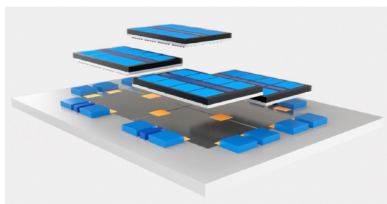
Through-silicon vias (TSVs) are vertical electrical interconnects that traverse through the silicon substrate, enabling multi-die stacking and 3D integration. TSVs facilitate the vertical integration of heterogeneous devices, such as logic, memory, and sensors, on a single silicon substrate, thereby reducing interconnect length, improving performance, and conserving space. TSVs are instrumental in advanced packaging technologies like 3D stacked memory, system-on-chip (SoC) integration, and interposer-based packaging, driving innovations in high-performance computing, artificial intelligence, and networking applications.
High Bandwidth Memory (HBM) is an advanced memory technology that leverages vertical stacking and TSVs to achieve unprecedented levels of memory bandwidth and energy efficiency. HBM utilizes multiple DRAM dies vertically stacked on top of each other and interconnected through TSVs, allowing for significantly higher memory bandwidth compared to traditional memory architectures. HBM is widely used in graphics cards, data centers, and highperformance computing systems, where memory bandwidth and power efficiency are critical for handling large datasets and complex workloads.
Chip-on-Wafer-on-Substrate (CoWoS) is a packaging technology developed by TSMC that enables the integration of multiple silicon dies on a single substrate, or interposer. In CoWoS, individual chips are fabricated on separate wafers and then bonded onto a silicon interposer using microbumps and TSVs. This allows for heterogeneous integration of different functional blocks, such as logic, memory, and analog, on a single package, enabling higher levels of performance, power efficiency, and system-level integration. CoWoS is widely used in highperformance computing, networking, and AI accelerators, where heterogeneous integration is essential for achieving optimal performance and functionality.
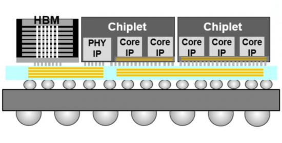
Foveros is an advanced packaging technology developed by Intel that enables 3D stacking of logic dies, memory dies, and other components to create highly integrated and compact semiconductor packages. In Foveros, individual dies are fabricated separately and then stacked vertically using microbumps and TSVs, allowing for dense integration of heterogeneous components with minimal footprint. Foveros enables innovative form factors, such as chiplets and system-in-package (SiP), and facilitates the development of power-efficient, highperformance devices for a wide range of applications, including mobile computing, IoT, and edge computing.
Investing in a semiconductor advanced packaging report offers several compelling reasons, each of which contributes to enhancing your understanding of the industry and making informed decisions. Here's why you should consider purchasing such a report:
Industry Insights: A semiconductor advanced packaging report provides comprehensive insights into the latest trends, developments, and innovations shaping the semiconductor packaging landscape. It offers valuable information on emerging technologies, market dynamics, and competitive landscape, helping you stay updated with the latest industry advancements.
Market Analysis: The report offers in-depth analysis of the semiconductor packaging market, including market size, growth potential, and key drivers and challenges. It provides detailed segmentation by packaging type, application, and region, for FOWLP, through-silicon vias (TSVs), and 3D integration, as well as AI-based technologies including HBM3, CoWoS, and Foveros.
Competitive Intelligence: By examining the strategies, product portfolios, and market positioning of key players in the semiconductor packaging industry, the report offers valuable competitive intelligence. It helps you benchmark your company's performance against industry leaders, identify potential collaborators or acquisition targets, and develop effective market entry or expansion strategies.
Technology Trends: Semiconductor advanced packaging reports delve into the latest technological advancements and innovations in packaging techniques such as fan-out waferlevel packaging (FOWLP), through-silicon vias (TSVs), and 3D integration, as well as AI-based technologies including HBM3, CoWoS, and Foveros. By understanding the evolving technological landscape, you can anticipate future trends, align your R&D efforts with market demands, and gain a competitive edge in the industry.
Investment Opportunities: Armed with comprehensive market insights and competitive analysis, a semiconductor advanced packaging report enables you to identify attractive investment opportunities across different segments of the semiconductor packaging market. Whether you're a semiconductor manufacturer, equipment supplier, or investor, the report provides valuable guidance for making strategic investment decisions and maximizing returns on investment.