3D TSV 및 2.5D 시장 : 시장 점유율 분석, 산업 동향 및 통계, 성장 예측(2025-2030년)
3D TSV And 2.5D - Market Share Analysis, Industry Trends & Statistics, Growth Forecasts (2025 - 2030)
상품코드:1651039
리서치사:Mordor Intelligence
발행일:2025년 02월
페이지 정보:영문
라이선스 & 가격 (부가세 별도)
ㅁ Add-on 가능: 고객의 요청에 따라 일정한 범위 내에서 Customization이 가능합니다. 자세한 사항은 문의해 주시기 바랍니다.
ㅁ 보고서에 따라 최신 정보로 업데이트하여 보내드립니다. 배송기일은 문의해 주시기 바랍니다.
한글목차
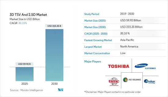
3D TSV 및 2.5D 시장 규모는 2025년에 599억 2,000만 달러로 추정되고, 예측 기간(2025-2030년)의 CAGR은 30.1%로 전망되며, 2030년에는 2,233억 5,000만 달러에 달할 것으로 예측됩니다.
반도체 산업의 패키징은 지속적인 변화를 겪고 있습니다. 반도체 용도의 성장과 함께 CMOS 스케일링의 둔화와 가격 상승으로 산업은 IC 패키징의 선진에 의존할 수밖에 없습니다. 3D 라미네이션 기술은 AI, ML, 데이터센터와 같은 용도의 요구 성능을 충족하는 솔루션입니다. 따라서 고성능 컴퓨팅 용도에 대한 요구가 증가함에 따라 예측 기간 동안 주로 TSV(Through Silicon Via) 시장을 견인하고 있습니다.
주요 하이라이트
3D TSV 패키징 기술도 견인역이 되고 있습니다. 현재의 와이어 본딩 기술에 비해 칩 간의 데이터 전송 시간이 단축되므로 고속화와 함께 전력 소비가 크게 줄어듭니다. 2022년 10월, TSMC는 독창적인 3DFabric 얼라이언스의 출시를 발표했습니다. 이는 TSMC의 개방형 혁신 플랫폼(OIP)에 해당하는 소개이며, 고객이 급증하는 반도체 및 시스템 레벨 설계 문제의 장애물을 극복하는 데 도움이 됩니다. 또한 TSMC의 3DFabric 기술을 이용한 차세대 HPC와 모바일 기술의 진보의 신속한 통합에 기여합니다.
전자기기에 대한 소비자 수요 증가는 다양한 새로운 기능을 실현하는 선진적 반도체 디바이스의 필요성에 불을 붙였습니다. 반도체 장비에 대한 요구가 지속적으로 강화됨에 따라 고급 패키징 기술은 오늘날의 디지털화된 세계에 필요한 폼 팩터와 처리 능력을 제공합니다. 예를 들어 반도체 산업 협회에 따르면 2022년 8월 세계 반도체 산업 매출은 474억 달러로 2021년 8월 총 473억 달러에서 0.1%의 미세 증가를 보였습니다.
또한 GSM 협회에 따르면 2025년까지 미국은 세계에서 가장 스마트폰 보급률이 높아질 것으로 예상되고 있습니다(연결의 49%). 미국 IoT 협회에 따르면 미국은 가구당 스마트 홈 디바이스 비율이 가장 높고 2개 또는 3개의 이용 사례(에너지, 보안, 소비자용 전자 기기)에 걸친 소비자용 전자 기기 제품을 소유하는 소비자의 추세가 가장 두드러집니다.
게다가 2022년 9월 바이덴 정권은 미국이 국가 안보에 필수적인 세계 최첨단 칩 생산량 제로, 소비량 25%이기 때문에 중국 의존에 대항하기 위해 국내 반도체 산업 육성에 500억 달러를 투자한다고 발표했습니다. 조 바이덴 대통령은 2022년 8월 중국에 대한 미국 경쟁 강화의 일환으로 국내 하이테크 제조업을 뒷받침하는 2,800억 달러의 CHIPS 법안에 서명했습니다. 이러한 반도체 부문에 대한 왕성한 투자는 연구 시장의 성장에 유리한 기회를 가져올 것으로 예상됩니다.
MEMS와 센서의 성장은 자동차나 산업 자동화 등 다양한 용도로 센서나 디스플레이 수요가 급속히 높아지고 있는 것에 기인하고 있습니다. 2022년 8월, MEMS의 제조업체이자 세계 반도체 산업의 중요한 진출기업인 STMicroelectronics는 소비자를 위한 스마트 산업, 모바일 기기, 의료 및 소매 부문을 위해 설계된 3세대 MEMS 센서를 발표했습니다. 견고한 칩 사이즈 모션 센서와 환경 센서는 오늘날 스마트폰의 사용자 친화적인 상황 인식 기능을 제공하며, 웨어러블 단말기는 MEMS 기술로 제작되었습니다. ST의 최신 MEMS 센서 세대는 출력 정밀도와 전력 소비에 관한 기술적 한계를 넓혀 성능을 새로운 수준으로 끌어올리고 있습니다.
또한 TSV 디바이스 제조와 관련된 높은 비용이 시장 성장을 제한하고 있습니다. 여기에는 장치 비용뿐만 아니라 장치가 제대로 작동하는 데 필요한 액세서리 및 소모품 비용도 포함됩니다. 또한 TSV 디바이스 제조에 대한 엄격한 지침과 규정도 비용에 박차를 가하고 있습니다.
게다가 세계 반도체 부족은 유행 후 생산 능력 확대에 주력하는 진출기업을 뒷받침했습니다. 예를 들어, SMIC은 다양한 도시에 독자적인 칩 제조 공장을 건설하고 2025년까지 생산 능력을 두 배로 늘리는 적극적인 계획을 발표했습니다. 또한 많은 아시아태평양 지방정부가 장기적인 프로그램으로 반도체 산업에 자금을 제공하고 있어 시장 성장 회복이 기대되고 있습니다. 예를 들어, 중국 정부는 국가 IC 투자 기금 2030의 두 번째 단계의 비용으로 약 230억-300억 달러를 도입했습니다.
또한, 현재 진행 중인 러시아와 우크라이나의 분쟁은 전자 산업에 큰 영향을 미칠 것으로 예상됩니다. 분쟁은 이미 산업에 영향을 미치는 반도체 공급망 문제와 칩 부족을 악화시키고 있습니다. 이 혼란은 니켈, 팔라듐, 구리, 티타늄, 알루미늄, 철광석과 같은 중요한 원료의 가격 변동의 형태로 나타나며 재료 부족을 초래할 수 있습니다. 그 결과, 3D 적층 메모리의 제조가 방해받게 됩니다.
3D TSV 및 2.5D 시장 동향
LED 패키징이 현저한 성장을 이룰 전망
LED 제품에 대한 사용이 증가하여 고출력, 고밀도 및 저비용 장치의 확대가 촉진되었습니다. 실리콘 관통 전극(TSV) 기술을 사용한 3차원(3D) 패키징은 2D 패키징과 달리 고밀도 수직 상호 연결을 가능하게 합니다.
TSV 집적 회로는 연결 길이를 줄여 기생 커패시턴스, 인덕턴스 및 저항을 줄이고 모놀리식 집적과 다기능 집적의 조합을 효율적으로 수행하여 빠르고 저전력 인터커넥트를 가능하게 합니다. IEA에 따르면 국제 조명 시장에서 LED의 보급률은 2025년에는 약 76%에 달하고, 2030년에는 87.4%에 이를 것으로 예상됩니다.
또한, 에너지 효율적인 LED를 채용하기 위한 정부의 이니셔티브와 규칙이 조사된 시장을 견인하고 있습니다. 국제에너지기구(IEA)에 따르면 조명시장에서 LED의 성장률은 2025년 75.8%가 될 것으로 예상되고 있습니다.
LED 패키징 요구 사항은 더 나아질 수 있습니다. LED 칩의 패키징 위치가 정확하지 않으면 패키징 장비 전체의 발광 효율이 직접 영향을 받을 수 있습니다. 정해진 위치에서 벗어나면 LED 빛이 반사 컵에서 완전히 반사되지 않고 LED 밝기에 영향을 미칩니다.
미국 에너지부는 최근 최신 기술을 이용한 10개 검사 프로젝트에 6,100만 달러를 투자해 수천 개의 가정과 기업을 최첨단 에너지 효율적인 네트워크로 전환할 것이라고 발표했습니다. 이는 백열 전구와 할로겐 전구를 보다 에너지 효율적인 LED 조명으로 전환하는 데에도 적용됩니다. 결과적으로 LED가 확대됨에 따라 미국의 LED 패키징 요구는 예측 기간 동안 성장합니다.
게다가 시장의 다양한 진출 기업들이 조사된 시장에서 신제품을 개발하고 있습니다. 2022년 5월 Lumileds LLC는 고전력 CSP(칩 스케일 패키징) LED를 출시했습니다. LUXEON HL1Z는 돔형이 아닌 편면 발광으로, 불과 1.4mm각의 작은 박스로부터 높은 발광 효율(137lm/W이상)을 실현합니다.
LED 패키징 용도의 급속한 발전으로 향후 몇 년동안 기술 혁신과 소비가 증가하고 조사된 시장 성장이 촉진될 것으로 예측됩니다. 한편, 포화도가 높기 때문에 제품의 수용이 제한될 수 있어 시장 성장이 제한됩니다.
아시아태평양이 큰 시장 점유율을 차지할 전망
아시아태평양은 본 시장에서 현저한 성장을 이루고 있는 지역입니다. 스마트폰의 보급률이 높아짐에 따라 이 지역은 세계 주요 모바일 시장 중 하나가 되었습니다.
GSM 협회에 따르면 스마트폰의 광대역 네트워크는 아시아태평양 인구의 96%를 커버하며 12억 명이 모바일 인터넷 서비스에 액세스하고 있다고 합니다. 5G의 기세는 아시아 전역에서 계속되고 있으며 현재 14개 시장에서 상용 5G 서비스를 이용할 수 있습니다. 인도와 베트남을 포함한 몇몇 다른 시장에서도 향후 몇 년동안 상용 서비스가 시작될 것으로 예상됩니다. 2025년까지 이 지역 전체에서 4억개의 5G 연결이 예상되며 이는 인구의 14% 이상에 해당합니다. 또한 인더스트리 4.0도 아시아태평양의 가장 새로운 동향 중 하나입니다. IoT 디바이스와 소형화는 3D TSV를 활용한 Industry 4.0의 중요한 동향입니다. 이 지역은 스마트 시티 인프라를 지원하기 위해 IoT에 상당한 투자를 하고 있습니다.
기술의 개발은 소비자용 전자기기, 통신, 의료기기, 통신기기, 자동차의 발전에 공헌하고 있습니다. 이 나라에서는 5G의 혜택이 개시되어, 특히 스마트폰 수요가 높아지고 있습니다.
MIIT에 따르면 중국은 차세대 모바일 네트워크를 개발하기 위해 2022년 200만 5G 기지국 설치를 원한다고 밝혔습니다. MIIT에 따르면 중국 본토에는 현재 142만 5,000개의 설치된 5G 기지국이 있으며, 전국에서 5억 명 이상의 5G 사용자를 지원하고 있으며 세계에서 가장 종합적인 네트워크가 되고 있습니다. 이 지역에서의 5G 도입 확대는 5G 대응 디바이스 수요를 촉진하여 2.5D 및 3D 반도체 패키징의 필요성을 높일 것으로 예상됩니다.
또한 CAICT에 따르면 5G 스마트폰 출하 대수는 국내 출하 대수의 75.9%로 성장을 지속하고, 있으며, 세계 평균의 40.7%보다 크다고 합니다. 2022년 7월까지 5G 스마트폰은 중국의 모든 휴대전화 출하량의 74%에 이를 것으로 예상됩니다. 2022년 7월까지 5G 휴대전화의 총 출하 대수는 124mm대로 중국은 121기종의 최신 5G 휴대전화를 도입했습니다. 이러한 추세는 이 지역의 2.5D 및 3D 반도체 패키징 솔루션 수요를 가속화할 것으로 예상됩니다.
자율주행차와 전기자동차의 이용 증가도 지역 전체의 첨단 반도체 수요를 증가시키고 있어 연구시장의 성장을 더욱 뒷받침하고 있습니다. 2022년 2월 Tesla는 중국 국내 및 수출 시장에서 수요 증가에 대응하기 위해 중국에 제2EV 시설을 건설할 예정입니다. 단기적으로 Tesla는 중국에서 생산 능력을 적어도 연간 100만대까지 끌어올릴 의향으로 상하이 린항 자유 무역구에 있는 현재 전시회 주변에 제2공장을 계획하고 있습니다. 게다가 중국 정부는 2025년까지 전차 판매 대수의 20%를 전기차로 하는 것을 목표로 하고 있으며, 여기에는 차세대 공용차로서 NEV를 채용하는 것도 포함됩니다.
게다가 반도체 제조와 패키징 공장에 대한 투자가 확대되고 있는 것도 조사 대상 시장에 유리한 성장 시나리오를 창출하고 있습니다. 예를 들어 선도적인 반도체 칩 제조업체 인 Intel은 최근 말레이시아에 고급 칩 패키징 시설을 건설하기 위해 70억 달러를 투자한다고 발표했습니다. 마찬가지로 2022년 11월 Advanced Semiconductor Engineering(ASE)은 말레이시아의 생산 기지 확대를 위해 3억 달러의 투자를 발표했습니다.
3D TSV 및 2.5D 산업 개요
3D TSV 및 2.5D 시장은 경쟁이 치열하고 다양해지기 때문에 다양한 중요한 연기자로 구성되어 있습니다. 시장에는 소규모, 대규모, 현지 벤더가 존재하며 우수한 경쟁을 창출하고 있습니다. 이러한 기업들은 시장 점유율을 확대하고 수익성을 높이기 위해 전략적 협력 관계를 구축하고 있습니다. 또한, 이 시장의 각사는 기업용 네트워크 기기 기술에 임하는 신흥 기업을 인수하여 제품력을 강화하고 있습니다.
2022년 8월-인텔은 2.5D 및 3D 기반 칩 설계를 지원하는 독자적인 아키텍처와 패키징의 혁신을 선보였으며, 칩 제조 기술과 그 중요성에 걸출한 시대의 도래를 알렸습니다. 인텔의 시스템 파운드리 모델의 특징은 패키징 강화입니다. 이 조직은 2030년까지 패키징 상의 트랜지스터 수를 1,000억 개에서 1조 개로 개선할 의향입니다.
2022년 3월-애플은 2.5D 접근법을 채택하여 칩렛을 이용한 미래의 설계에 문을 여는 최신 M1 Ultra 디바이스의 실현을 뒷받침했습니다. UltraFusion이라는 패키징 아키텍처는 실리콘 인터포저를 통해 2개의 M1 Max 칩의 다이를 상호 연결하여 1,140억 트랜지스터의 시스템 온 어 칩(SoC)을 구축합니다. 이는 실리콘 기판과 인터포저를 활용하여 2개의 다이 사이에 2.5TB/sec의 낮은 대기 시간과 프로세서 간 대역폭을 가진 10,000개의 상호 연결로 2개의 다이를 지원합니다. 또한 초당 800GB의 인터페이스에서 작동하는 128GB의 낮은 대기 시간 통합 메모리에 연결됩니다.
기타 혜택
엑셀 형식 시장 예측(ME) 시트
3개월간의 애널리스트 서포트
목차
제1장 서론
조사의 전제조건 및 시장의 정의
조사 범위
제2장 조사 방법
제3장 주요 요약
제4장 시장 인사이트
시장 개요
산업의 매력-Porter's Five Forces 분석
공급기업의 협상력
구매자의 협상력
신규 진입업자의 위협
대체품의 위협
경쟁 기업간 경쟁 관계의 강도
산업 밸류체인 분석
거시 경제 동향이 시장에 미치는 영향
제5장 시장 역학
시장 성장 촉진요인
고성능 컴퓨팅 애플리케이션 시장 확대
데이터센터와 메모리 디바이스 확대
시장의 과제
IC 패키징의 고단가화
제6장 기술 스냅샷
제7장 시장 세분화
패키징 유형별
3D 적층 메모리
2.5D 인터포저
TSV 부착 CIS
3D SoC
기타 패키징 유형(LED, MEMS 및 센서 등)
최종 사용자 용도별
소비자 전자기기
자동차
고성능 컴퓨팅(HPC)과 네트워킹
기타 최종 사용자 용도
지역별
북미
미국
캐나다
유럽
영국
독일
프랑스
이탈리아
기타 유럽
아시아태평양
중국
인도
일본
호주
동남아시아
기타 아시아태평양
기타
제8장 경쟁 구도
기업 프로파일
Toshiba Corp.
Samsung Electronics Co. Ltd.
ASE Group
Taiwan Semiconductor Manufacturing Company Limited
Amkor Technology, Inc.
Pure Storage Inc.
United Microelectronics Corp.
STMicroelectronics NV
Broadcom Ltd.
Intel Corporation
Jiangsu Changing Electronics Technology Co. Ltd.
제9장 투자 분석
제10장 시장의 미래
AJY
영문 목차
영문목차
The 3D TSV And 2.5D Market size is estimated at USD 59.92 billion in 2025, and is expected to reach USD 223.35 billion by 2030, at a CAGR of 30.1% during the forecast period (2025-2030).
Packaging in the semiconductor industry has noticed a continuous transformation. As the semiconductor applications are growing, the slowdown in CMOS scaling and escalating prices have forced the industry to rely on the advancement in IC packaging. 3D stacking technologies are the solution that meets the required performance of applications like AI, ML, and data centers. Therefore, the growing requirement for high-performance computing applications mainly drives the TSV (Through Silicon Via) market over the forecast period.
Key Highlights
The 3D TSV packaging technology is also achieving traction. It reduces data transmission time between chips and the current wire bonding technology, resulting in significantly lower power consumption with faster speed. In October 2022, TSMC announced the launch of the creative 3DFabric Alliance, a considerable introduction to TSMC's Open Innovation Platform (OIP) to help customers overcome the surging hurdles of semiconductor and system-level design challenges. It will also help in gaining rapid integration of advancements for next-generation HPC and mobile technologies using TSMC's 3DFabric technologies.
Increasing consumer demand for electronics has sparked the need for advanced semiconductor devices that enable various new capabilities. As the demands for semiconductor appliances intensify consistently, advanced packaging techniques deliver the form factor and processing power required for today's digitized world. For instance, according to the Semiconductor Industry Association, during August 2022, global semiconductor industry sales were USD 47.4 billion, a slight boost of 0.1% over the August 2021 total of USD 47.3 billion.
In addition, according to the GSM Association, by 2025, the United States is expected to have the highest smartphone adoption globally (49% of connections). As per the United States IoT Association, it has the highest smart home device ratio per household and the most significant consumer tendency to own appliances across two or three use cases (energy, security, and appliances).
Moreover, in September 2022, the Biden administration announced that it would invest USD 50 billion in building up the domestic semiconductor industry to counter dependency on China, as the US produces zero and consumes 25% of the world's leading-edge chips vital for its national security. President Joe Biden signed a USD 280 billion CHIPS bill in August 2022 to boost domestic high-tech manufacturing, part of his administration's push to increase US competitiveness over China. Such robust investments in the semiconductor sector would present lucrative opportunities for the growth of the studied market.
The growth of MEMS and Sensors is attributed to the rapidly increasing demand for sensors and displays in various applications such as automotive, industrial automation, and many others. In August 2022, STMicroelectronics, a maker of MEMS and a significant player in the worldwide semiconductor industry, launched its third generation of MEMS sensors designed for consumer smart industries, mobile devices, healthcare, and retail sectors. The robust, chip-sized motion and environmental sensors power the user-friendly, context-aware features of today's smartphones, and wearables are made on MEMS technology. ST's most recent MEMS sensor generation drives technical boundaries regarding output accuracy and power consumption, elevating performance to a new level.
Furthermore, the high costs associated with TSV device manufacturing restrict market growth. This includes not only the cost of devices but also the cost of accessories and consumables needed for their proper functioning. Moreover, the stringent guidelines and regulations governing TSV device manufacturing also add to the charges.
Furthermore, the worldwide semiconductor shortage encouraged players to focus on expanding production capacity during a post-pandemic. For instance, the SMIC announced aggressive plans to double its production capacity by 2025 by constructing unique chip fabrication plants in different cities. Also, many Asian-Pacific local governments have funded the semiconductor industry in a long-term program, hence anticipated to regain market growth. For instance, the Chinese government introduced roughly USD 23-30 billion to pay for the second stage of its National IC Investment Fund 2030.
Moreover, the ongoing conflict between Russia and Ukraine is expected to impact the electronics industry significantly. The conflict has already exacerbated the semiconductor supply chain issues and the chip shortage that have affected the industry for some time. The disruption may come in the form of volatile pricing for critical raw materials such as nickel, palladium, copper, titanium, aluminum, and iron ore, resulting in material shortages. This would obstruct the manufacturing of 3D Stacked Memory.
3D TSV And 2.5D Market Trends
LED Packaging Expected to Witness the Significant Growth
The increasing use of LED in products has promoted the expansion of higher power, greater density, and lower-cost devices. Using three-dimensional (3D) packaging through silicon via (TSV) technology authorizes a high density of vertical interconnects, unlike 2D packaging.
TSV integrated circuits reduce connection lengths; thus, smaller parasitic capacitance, inductance, and resistance are required where a combination of monolithic and multifunctional integration is done efficiently, providing high-speed, low-power interconnects. According to IEA, the penetration rate of LEDs into the international lighting market is expected to reach some 76% in 2025 and further to 87.4% in 2030.
Further, government initiatives and rules to adopt energy-efficient LEDs drive the studied Market. According to the International Energy Agency (IEA), the growth rate of LEDs in the lighting market is anticipated to be 75.8% in 2025.
The requirements for LED packaging could be much better. If LED chips are not positioned into the package precisely, the luminescence efficiency of the overall packaging appliance might be affected directly. Any deviation from the established position will prevent LED light from being fully reflected from the reflective cup, affecting the LED's brightness.
The US Department of Energy recently announced investing USD 61 million in 10 pilot projects using the latest technologies to turn thousands of homes and businesses into cutting-edge, energy-efficient networks. This applies to switching out incandescent and halogen bulbs for better energy-efficient LED lighting. As a result, with the expansion in LEDs, the LED packaging need in the United States will grow in the forecasted period.
Furthermore, various players in the market are developing new products in the studied Market. In May 2022, Lumileds LLC launched high-power CSP (chip-scale package) LED. The LUXEON HL1Z is an un-domed, single-sided emitter that delivers high luminous efficacy (137lm/W or more) from a tiny box, just 1.4mm square.
Rapid advancements in LED package applications are projected to raise innovation and consumption in the coming years, propelling the studied market growth. On the other hand, high saturation may limit product acceptance, which, in turn, limits market growth.
Asia-Pacific is Expected to Hold the Significant Market Share
Asia-Pacific is the significant-growing region in the Market studied. The rising smartphone adoption rates have made the region one of the major mobile markets in the world, primarily due to the increasing population evolution and urbanization.
As per the GSM Association, smartphone broadband networks cover 96% of the population of APAC, with 1.2 billion people accessing mobile internet services. 5G momentum continues revving across the region, with commercial 5G services currently available across 14 markets. Several others, including India and Vietnam, are expected to board in the coming years. By 2025, there will be 400 million 5G connections across the region, over 14% of the population. Further, industry 4.0 is also one of Asia-Pacific's most emerging trends. IoT devices and miniaturization are important trends in Industry 4.0, utilizing 3D TSV. The region is investing heavily in IoT to support smart city infrastructure.
Advancing technologies have contributed to the development of consumer electronics, telecom, medical devices, communication devices, and automotive. With the launch of 5G benefits in the country, the demand for smartphones, among other things, has been rising.
According to the MIIT, China desired 2 million installed 5G base stations in 2022 to develop the country's next-generation mobile network. The Chinese mainland presently has 1.425 million installed 5G base stations that support more than 500 million 5G users nationally, making it the most comprehensive network in the world, as per MIIT. The growing implementation of 5G in the region is also expected to promote the demand for 5G-enabled devices, thereby increasing the need for 2.5D and 3D semiconductor packaging.
Further, according to CAICT, 5G smartphone shipments are recorded for 75.9% of domestic shipments, more significant than a global average of 40.7%. By July 2022, 5G smartphones will have reached 74% of all cellphone shipments in China. The total number of 5G cell phone shipments by July 2022 was 124mm units, and China introduced 121 latest 5G mobile phone models. Such trends would accelerate the region's demand for 2.5D and 3D semiconductor packaging solutions.
The increasing use of autonomous and electric vehicles has also increased the demand for advanced semiconductors across the region, further supporting the studied Market's growth. In February 2022, Tesla plans to build a 2nd EV facility in China to keep up with rising demand locally and in export markets. In the short term, Tesla intends to increase capacity in China to at least 1mm cars yearly, with a second plant planned around its present exhibition in Shanghai's Lingang free trade zone. In addition, the Chinese government seeks 20% of all vehicle sales to be electric by 2025, including adopting NEVs as the next generation of government vehicles.
Moreover, the growing investments in semiconductor manufacturing and packaging plants also create a favorable growth scenario for the studied Market. For instance, Intel, a significant semiconductor chip manufacturer, recently announced a USD 7 billion investment to build an advanced chip packaging facility in Malaysia. Similarly, in November 2022, Advanced Semiconductor Engineering (ASE) announced a USD 300 million investment to expand its production site in Malaysia.
3D TSV And 2.5D Industry Overview
The 3D TSV and 2.5D market is highly competitive and consists of various significant performers as it is diversified. The existence of small, large, and local vendors in the Market creates excellent competition. These firms leverage strategic collaborative endeavors to expand their market share and increase profitability. The companies in the Market are also acquiring start-ups performing on enterprise network equipment technologies to strengthen their product capabilities.
In August 2022, Intel showcased the unique architectural and packaging breakthroughs that help 2.5D and 3D-based chip designs, ushering in a remarkable era in chipmaking technologies and their importance. Intel's system foundry model features enhanced packaging. The organization intends to improve the number of transistors on a package from 100 billion to 1 trillion by 2030.
In March 2022, Apple adopted a 2.5D approach to boost the enactment of its latest M1 Ultra device that unlocks the door to future designs utilizing chiplets. A packaging architecture called UltraFusion interconnects the die of two M1 Max chips on a silicon interposer to build a system on a chip (SoC) with 114bn transistors. This utilizes a silicon substrate and interposer that supports the two dies with 10,000 interconnects with 2.5 TB/s of low latency and inter-processor bandwidth between the die. This also connects the die to 128 GB of low-latency unified memory operating an 800 GB/s interface.
Additional Benefits:
The market estimate (ME) sheet in Excel format
3 months of analyst support
TABLE OF CONTENTS
1 INTRODUCTION
1.1 Study Assumptions and Market Definitions
1.2 Scope of the Study
2 RESEARCH METHODOLOGY
3 EXECUTIVE SUMMARY
4 MARKET INSIGHTS
4.1 Market Overview
4.2 Industry Attractiveness - Porter's Five Forces Analysis
4.2.1 Bargaining Power of Suppliers
4.2.2 Bargaining Power of Buyers
4.2.3 Threat of New Entrants
4.2.4 Threat of Substitute Products
4.2.5 Intensity of Competitive Rivalry
4.3 Industry Value Chain Analysis
4.4 Impact of Macroeconomic Trends on the Market
5 MARKET DYNAMICS
5.1 Market Drivers
5.1.1 Expanding Market for High Performance Computing Application
5.1.2 Expanding Scope of Data Centers and Memory Devices
5.2 Market Challenges
5.2.1 High Unit Cost of IC Packages
6 TECHNOLOGICAL SNAPSHOT
7 MARKET SEGMENTATION
7.1 By Packaging Type
7.1.1 3D Stacked Memory
7.1.2 2.5D Interposer
7.1.3 CIS with TSV
7.1.4 3D SoC
7.1.5 Other Packaging Types ( LED, MEMS & Sensors, etc.)
7.2 By End User Application
7.2.1 Consumer Electronics
7.2.2 Automotive
7.2.3 High Performance Computing (HPC) and Networking
7.2.4 Other End User Applications
7.3 By Geography
7.3.1 North America
7.3.1.1 U.S.
7.3.1.2 Canada
7.3.2 Europe
7.3.2.1 United Kingdom
7.3.2.2 Germany
7.3.2.3 France
7.3.2.4 Italy
7.3.2.5 Rest of Europe
7.3.3 Asia-Pacific
7.3.3.1 China
7.3.3.2 India
7.3.3.3 Japan
7.3.3.4 Australia
7.3.3.5 South East Asia
7.3.3.6 Rest of Asia-Pacific
7.3.4 Rest of the World
8 COMPETITIVE LANDSCAPE
8.1 Company Profiles
8.1.1 Toshiba Corp.
8.1.2 Samsung Electronics Co. Ltd.
8.1.3 ASE Group
8.1.4 Taiwan Semiconductor Manufacturing Company Limited