


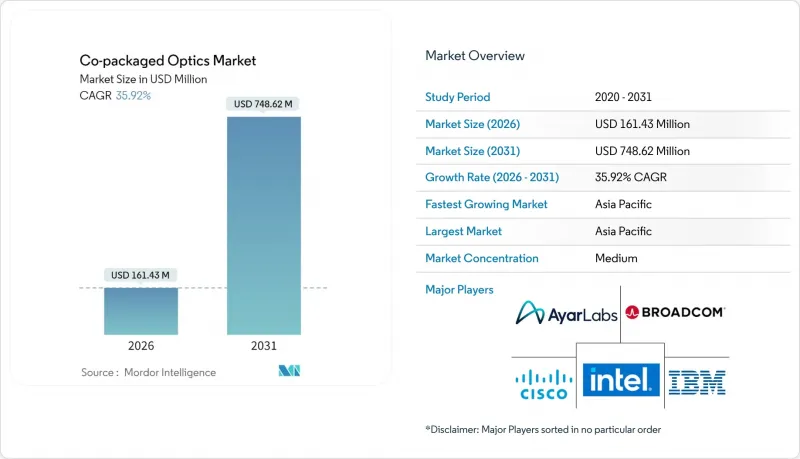
공동 패키지 광학(CPO) 시장은 2025년에 1억 2,000만 달러로 평가되었으며, 2026년 1억 6,000만 달러에서 2031년까지 7억 5,000만 달러에 달할 것으로 예측됩니다.
예측 기간(2026-2031년) 동안 CAGR은 35.92%로 예상됩니다.
과거에는 주로 실험 단계에 머물렀던 실리콘 포토닉스 통합은 현재 대량 생산이 가능한 반도체 제조 기술과 첨단 패키징 기술의 혜택을 받아 하이퍼스케일 사업자가 51.2 Tbps 스위치 실리콘에 필적하는 대역폭 밀도를 구현하면서 전력 소비를 줄일 수 있게 되었습니다. 전력 소비를 줄일 수 있습니다. (1) AI 트레이닝 클러스터는 기존 클라우드 아키텍처보다 훨씬 더 고밀도의 동서방향 대역폭을 필요로 하고, (2) 북미와 EU의 에너지 효율화 요구로 인해 와트/기가비트 지표를 낮추는 솔루션이 선호되고, (3) 파운더의 진입, 특히 TSMC의 실리콘 포토닉스 패키징 프로그램으로 인해 광 레인당 비용 절감 및 수율 향상에 기여하고 있습니다. (3) 파운드리 업체(특히 TSMC의 실리콘 포토닉스 패키징 프로그램)의 진입으로 광레인당 비용 절감과 수율 향상이 이루어질 것으로 예상됩니다. 광부품 공급업체, 반도체 제조업체, 신흥 실리콘 포토닉스 전문업체들이 공급 제약요인인 이종 통합 문제를 해결하기 위해 경쟁하는 가운데, 경쟁은 여전히 치열합니다. 오픈컴퓨팅 커뮤니티가 인터페이스 사양을 개선함에 따라, 코패키지드 옵틱스 시장은 얼리 어답터 단계에서 데이터센터 인프라의 주류로 전환될 것으로 예상됩니다.
브로드컴의 Bailly 플랫폼은 Tomahawk 5 스위치에 8개의 6.4Tbps 광엔진을 내장하여 플러그형 트랜시버 대비 70%의 저전력 소비를 실현한 것으로 나타났습니다. 하이퍼스케일 사업자들은 기존의 전기 배선이 51.2Tbps ASIC이 요구하는 신호 무결성을 유지할 수 없기 때문에 네트워크 토폴로지를 재평가해야 했습니다. 800G 플러그인형 디바이스의 랙 레벨 열 설계 예산이 실용적인 한계에 도달함에 따라 경제적 격차가 확대되고, 조달 부서는 CPO를 실험 프로젝트가 아닌 필수 기술로 취급하게 되었습니다. 3세대 200Gbit/s 레인을 탑재한 CPO가 양산 단계에 진입함에 따라, 코패키지 광학 시장은 2026년부터 2028년까지의 스위치 실리콘 업데이트 주기와 일치하는 명확한 기술 로드맵을 확보하게 되었습니다. 이를 통해 장비 OEM 업체들은 설계 채택을 가속화하고 중기 수요 가시성을 확보할 수 있게 되었습니다.
주요 클라우드 제공업체들의 넷제로 공약 발표 이후, 기가비트당 전력 소비량 지표에 대한 관심이 높아졌습니다. ASE의 5pJ/비트 미만의 광학 엔진은 스위치 패키지 내 광학 부품의 통합이 DSP의 전력 소비를 줄이고 구리 배선 손실을 제거한다는 것을 입증했습니다. EU의 탄소 가격제부터 도시 차원의 신규 데이터센터 건설 모라토리엄에 이르기까지 규제 압력으로 인해 전력 절감은 기판 차원의 과제가 되었습니다. 각 사업자들은 에너지 절감과 연동된 3년간의 투자 회수 목표를 제시함과 동시에, 사이트 전력 할당량을 초과하지 않고 랙 밀도 향상을 실현하기 위한 수단으로 코패키지드 광모듈 도입을 추진하고 있습니다. 이러한 정책적 환경은 기술적 우위가 투자의 필수 요건으로 전환되어 장기 구매 계약을 통한 수요 확대를 촉진하고 있습니다.
CPO(Co-Packaged Optics)는 실리콘 포토닉스, III-V 계열 레이저, 첨단 기판을 밀리미터 단위의 인클로저에 통합하는 기술입니다. 광도파로를 수십 나노미터의 정밀도로 정렬하면서 고출력 스위치 다이를 접합하는 공정에서는 여러 공정 단계에서 손실이 발생합니다. NVIDIA의 Blackwell 양산 확대 시 드러난 고급 CoWoS 라인의 수율 저하는 공정 윈도우의 취약점을 부각시키고 있습니다. 재료 불일치로 인한 열 응력 대책으로 특수한 계면층과 능동 냉각이 필요하며, 부품 수와 검사 공정이 증가합니다. 학습 곡선이 성숙하기 전까지는 양산 공급이 제한되고, 2차 OEM의 리드타임이 길어질 것으로 예상되며, 코패키지 광학 시장의 단기 출하량 예측은 억제될 것으로 보입니다.
2025년 공동 밀봉 광학 부품 시장 매출 중 3.2 Tbps 부문이 37.92%를 차지할 것으로 예상됩니다. 이는 Tomahawk 4 클래스 스위치의 도입 기반을 반영합니다. 그러나 AI 클러스터가 높은 라딕스 패브릭을 요구하는 가운데, 6.4Tbps 이상의 디바이스는 2031년까지 CAGR 58.64%로 성장할 것으로 예상됩니다. 6.4 Tbps 엔진 1기를 51.2 Tbps ASIC과 공배치하여 각 200 Gbit/s의 광레인 8개를 구현합니다. 이를 통해 스위치에서 모듈로의 전력 예산을 절반으로 줄이고, 리타이머 단계가 필요하지 않습니다. 각 벤더들은 2026년 이후 서버 업데이트 주기에 맞춰 6.4Tbps 이상의 로드맵을 확정하고 있습니다.
향후 파운더리의 로드맵에는 하나의 패키지에 여러 개의 광 코어를 적층하는 12.8Tbps 엔진이 계획되어 있어, 최상위 대역이 다른 모든 데이터 속도 계층을 능가하는 성장이 예상됩니다. 1.6Tbps 미만의 CPO는 비용보다 밀도가 우선시되는 엣지 어플라이언스에는 여전히 유효하지만, 하이퍼스케일 입찰 문서에서는 현재 200G/레인의 신호 경로를 기준으로 규정되어 있습니다. 이러한 전환이 진행됨에 따라, 6.4Tbps 이상의 디바이스용 코패키지 옵틱 시장 규모는 2029년까지 저속 클래스를 합친 시장 규모를 넘어설 것으로 예상됩니다.
2025년 매출에서 광학 엔진은 41.12%를 차지했지만, 업체들이 온칩 발광 기술을 습득함에 따라 레이저 소스는 43.71%의 CAGR로 확대되고 있습니다. 중국산 200mm 실리콘 웨이퍼에서 제조되는 집적형 인듐 인화물 레이저 어레이는 외부 펌프 레이저의 필요성을 없애고 패키지 높이를 줄였습니다. 이를 통해 재료비를 절감하고 신뢰성을 향상시켰습니다.
전자 IC는 컨트롤러 기능의 패키지 내 집적화로 안정적인 수요를 유지하고 있지만, 부가가치의 원천은 레이저 기술 혁신으로 옮겨가고 있습니다. 통합 광원을 통해 파이버 피그 테일을 제거함으로써 시스템 설계자는 전면 패널의 공간을 확보할 수 있는 더 얇은 상단 블랙 스위치를 구현할 수 있습니다. 따라서 하이퍼스케일러와 레이저 파운더리 간의 다년간의 공급 계약에 힘입어 레이저 장치용 코패키지 광학 시장 규모는 틈새 시장에서 핵심 시장으로 이동하고 있습니다.
공동 패키지 광학(CPO) 시장은 데이터 속도(1.6T 미만, 1.6T, 3.2T 이상), 구성요소(광엔진, 전기 IC, 레이저 소스, 커넥터, 패키징 등), 통합 접근 방식(온보드 광학, 공동 패키지 광학), 최종 용도(하이퍼스케일러, 데이터센터, 통신사, 엔터프라이즈, 통신사, 기업, 기타)(하이퍼스케일러, 데이터센터, 통신사업자, 엔터프라이즈, 기타), 지역(아메리카, 유럽, 아시아태평양, 중동 및 아프리카)으로 세분화됩니다.
아시아태평양은 2025년 매출의 32.78%를 차지하며, 정부 보조금과 수직 통합 공급망에 힘입어 41.99%의 CAGR로 성장하고 있습니다. 중국의 82억 위안(약 1,300억 원)의 보조금으로 8인치 실리콘 포토닉스 웨이퍼 생산과 레이저 통합이 가능해져 부품 원가를 절감할 수 있게 되었습니다. 일본 경제산업성은 NTT, 인텔, SK하이닉스의 광칩 공동개발에 3억 5천만 달러를 출자하여 국내 설계 생태계를 강화하기 위해 노력하고 있습니다. 한국은 고대역폭 메모리 로드맵을 광 인터페이스와 연계하여 이 연계를 보완하고 있습니다.
북미에서는 하이퍼스케일 사업자를 통해 최종사용자 수요의 대부분을 공급하고 있습니다. 브로드컴, 인텔, 엔비디아와 함께 지역 기술 기반을 지원하고, TSMC의 애리조나 공장은 국내 패키징 능력을 도입하여 미국 클라우드 고객의 리드타임을 단축하고 있습니다. 따라서 칩 설계와 자체 소비를 연결하는 폐쇄형 루프는 공동 패키징 광학 부품 시장의 혜택을 누리고 있으며, 생산이 전 세계로 분산되는 가운데서도 이 지역의 점유율을 강화하고 있습니다.
유럽에서는 상호운용성과 지속가능성을 우선시합니다. EU에 본부를 둔 Open Compute Project의 지부가 인터페이스 설계안을 수립하고, 전 세계 도입 관행을 형성하고 있습니다. 탄소가격제는 도입을 더욱 촉진하고 있으며, 사업자들은 플러그인형 광모듈에서 코패키지 드레인으로의 전환을 통해 30-50%의 전력 절감 효과를 확인하고 있습니다. 노키아의 인피네라(Infinera) 23억 달러 인수로 대표되는 M&A 활동은 이 지역이 독자적인 광통신 지적재산을 확보하고 가치사슬의 업스트림로 진출하려는 의지를 보여주고 있습니다.
The co-packaged optics market was valued at USD 0.12 billion in 2025 and estimated to grow from USD 0.16 billion in 2026 to reach USD 0.75 billion by 2031, at a CAGR of 35.92% during the forecast period (2026-2031).

Silicon photonics integration, once largely experimental, now benefits from high-volume semiconductor manufacturing and advanced packaging, enabling hyperscale operators to pursue bandwidth densities that match 51.2 Tbps switch silicon while lowering power budgets. Growth momentum stems from three reinforcing trends: (1) AI training clusters require far denser east-west bandwidth than classic cloud architectures, (2) energy-efficiency mandates in North America and the EU prioritize solutions that trim watt-per-gigabit metrics, and (3) foundry participation-most visibly TSMC's silicon-photonics packaging programs-reduces cost per optical lane and improves yield. Competitive intensity remains high as optical component vendors, semiconductor houses, and new silicon-photonics specialists race to solve heterogeneous-integration challenges that still constrain supply. As open compute communities refine interface specifications, the co-packaged optics market is positioned to shift from early adopter status to mainstream data-center infrastructure.
Broadcom's Bailly platform showed how embedding eight 6.4 Tbps optical engines beside a Tomahawk 5 switch delivered 70% lower power draw than pluggable transceivers. Hyperscale operators consequently reassessed network topologies because legacy electrical traces could not sustain the signal integrity demanded by 51.2 Tbps ASICs. The economic gap widened when rack-level thermal budgets for 800G pluggables hit practical ceilings, prompting procurement teams to treat co-packaged optics as a necessity rather than a lab project. As the third-generation CPO with 200 Gbit/s lanes enters production, the co-packaged optics market gains a clear technical roadmap that aligns with 2026-2028 switch-silicon refresh cycles. Equipment OEMs, therefore, accelerate design wins, locking in demand visibility over the medium term.
Net-zero pledges published by major cloud providers intensified scrutiny on watts-per-gigabit metrics. ASE's demonstration of <5 pJ/bit optical engines confirmed that integrating optics inside the switch package cuts DSP power and eliminates copper trace losses. Regulatory pressure-from carbon-pricing schemes in the EU to city-level moratoriums on new data-center builds-made the power reduction a board-level issue. Operators outlined three-year payback targets tied to energy savings and, in parallel, positioned co-packaged optics as a lever to unlock higher rack densities without breaching site power envelopes. The policy environment, therefore, transforms a technical benefit into an investment imperative, boosting demand through long-term purchase agreements.
Co-packaged optics combines silicon photonics, III-V lasers, and advanced substrates inside a millimeter-scale envelope. Aligning optical waveguides to within tens of nanometers while also attaching high-power switch dice drives yields loss across multiple process steps. Recent yield slippages in advanced CoWoS lines, highlighted during NVIDIA's Blackwell ramp, underscore the fragile process window. Material-mismatch thermal stress necessitates exotic interface layers and active cooling, increasing part counts and inspection steps. Until learning curves mature, volume availability remains constrained, elongating lead times for tier-two OEMs and tempering near-term shipment forecasts for the co-packaged optics market.
Other drivers and restraints analyzed in the detailed report include:
For complete list of drivers and restraints, kindly check the Table Of Contents.
The 3.2 Tbps segment accounted for 37.92% of the co-packaged optics market revenue in 2025, reflecting the installed base of Tomahawk 4 class switches. However, >=6.4 Tbps devices are posting a 58.64% CAGR through 2031 as AI clusters press for higher radix fabrics. A single 6.4 Tbps engine co-located with a 51.2 Tbps ASIC yields eight optical lanes at 200 Gbit/s each, which halves the switch-to-module power budget and eliminates retimer stages. Vendors thus lock the >=6.4 Tbps roadmap into server refresh cycles beginning in 2026.
Looking forward, the foundry roadmaps project 12.8 Tbps engines that stack multiple optical cores within one package, positioning the top-end band to outgrow all other data-rate tiers. While sub-1.6 Tbps CPO remains viable for edge appliances where cost outranks density, hyperscale bidding documents now stipulate 200G/lane signal paths as a baseline. As this migration unfolds, the co-packaged optics market size for >=6.4 Tbps devices is set to outstrip the combined value of lower speed classes by 2029.
Optical engines represented 41.12% of 2025 revenue, yet laser sources are expanding at a 43.71% CAGR as vendors master on-chip light generation. China's integrated indium-phosphide laser arrays, produced on 200 mm silicon wafers, removed the need for external pump lasers and reduced package height, trimming material cost, and improved reliability.
Electronics ICs maintain steady demand as controller functions migrate on-package, but the incremental value pool is shifting toward laser innovation. With integrated sources eliminating fiber pigtails, system architects design slimmer top-of-rack switches and free front-panel real estate. The co-packaged optics market size for laser devices is therefore moving from niche to core, supported by multi-year supply agreements between hyperscalers and laser foundries.
Co-Packaged Optics Market is Segmented by Data Rate (< 1. 6T, 1. 6T, 3. 2T, and Above), Component (Optical Engine, Electrical IC, Laser Source, Connector and Packaging, and More), Integration Approach (On-Board Optics, and Co-Packaged Optics), End-Use Application (Hyperscale Cloud Data Centers, Enterprise Data Centers, and More), and Geography (North America, South America, Europe, Asia-Pacific, and Middle East and Africa).
Asia-Pacific commanded 32.78% of 2025 revenue and is advancing at a 41.99% CAGR, powered by government subsidies and vertically integrated supply. China's CNY 8.2 billion subsidy enabled eight-inch silicon-photonics wafer production and laser integration that compresses the bill-of-materials cost. Japan's Ministry of Economy, Trade and Industry funded USD 305 million for NTT, Intel, and SK Hynix to co-develop optical chips, strengthening local design ecosystems. South Korea complements the loop by aligning high-bandwidth memory roadmaps with optical interfaces.
North America supplies the bulk of end-user demand through hyperscale operators. Broadcom, Intel, and NVIDIA anchor the regional technology stack, while TSMC's Arizona fabs introduce domestic packaging capacity that shortens lead times for US cloud customers. The co-packaged optics market, therefore, benefits from a closed loop that links chip design to captive consumption, reinforcing the region's share even as production diversifies globally.
Europe prioritizes interoperability and sustainability. Open Compute Project chapters headquartered in the EU draft interface blueprints, shaping global deployment practices. Carbon-pricing legislation further propels adoption; operators document 30-50% power savings when shifting from pluggable optics to co-packaged lanes. M&A activity, typified by Nokia's USD 2.3 billion acquisition of Infinera, signals the region's intent to secure proprietary optical IP and climb the value chain.