ㅁ Add-on 가능: 고객의 요청에 따라 일정한 범위 내에서 Customization이 가능합니다. 자세한 사항은 문의해 주시기 바랍니다.
ㅁ 보고서에 따라 최신 정보로 업데이트하여 보내드립니다. 배송기일은 문의해 주시기 바랍니다.
한글목차
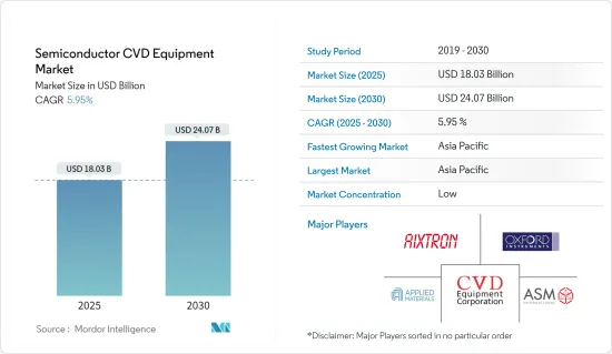
반도체 CVD 장비 시장 규모는 2025년에 180억 3,000만 달러, 2030년에는 240억 7,000만 달러에 이를 것으로 예측되며, 예측기간(2025-2030년)의 CAGR은 5.95%를 나타낼 전망입니다.
마이크로 일렉트로닉스 기반 소비자 제품에 대한 수요 증가로 인해 반도체, LED, 스토리지 디바이스 산업이 급성장하고 있으며, 전기도금용 Cr6의 사용에 대한 엄격한 규제가 주로 CVD 장비 시장의 성장을 견인하고 있습니다.
주요 하이라이트
화학 기상 성장(CVD) 공정은 반도체 제조 및 박막 제조에 자주 사용됩니다. 최근 CVD 합성은 2차원 재료의 무기 박막과 다양한 기판 상에 등각으로 증착할 수 있는 고순도 폴리머 박막을 모두 정밀하게 제조함으로써 새로운 높이에 도달하고 있습니다.
반도체 화학 기상 성장 장비 에서 전구체 가스(일반적으로 캐리어 가스로 희석된)는 거의 상온에서 반응 챔버로 공급됩니다. 이러한 가스는 가열된 기판을 통과하거나 접촉할 때 반응 또는 분해되어 기판 상에 증착되는 고상을 생성합니다. 기판의 온도는 발생하는 반응에 영향을 미치기 때문에 중요합니다.
CVD는 다결정, 단결정, 비정질, 에피택셜 등 다양한 형태의 재료를 증착하는 미세 가공 기술에 널리 사용되고 있습니다. 실리콘(이산화물, 탄화물, 질화물, 산질화물), 탄소(섬유, 나노섬유, 나노튜브, 다이아몬드, 그래핀), 플루오로카본, 필라멘트, 텅스텐, 티타늄 질화물, 다양한 고유전율 유전체 등이 이들 재료에 포함됩니다.
이러한 기술은 사물 인터넷 시장을 파괴하고 추진할 잠재력을 갖고 있기 때문에 신흥국 정부와 이해관계자들은 마이크로일렉트로닉스 업계 동향을 주시하고 있습니다. 가상현실과 증강현실 가제트의 채용이 증가하고 있기 때문에 다가오는 대역폭의 제약에 대응하여 마이크로 일렉트로닉스의 연구 개발도 증가할 가능성이 있습니다.
그들은 반도체를 만들고 있습니다. CVD 설정은 복잡하고 엄청난 비용이 듭니다. 주조 업체와 반도체 조립 및 테스트 회사(OSAT)는 칩 수요 증가에 대응하기 위해 생산 확대를 계속하고 있기 때문에 설비 투자에 대한 압력이 높아질 가능성이 높습니다.
COVID-19의 발생은 반도체 칩 제조 시장 전체에 수요 및 공급의 양면으로부터 영향을 주었습니다. 전국적인 반도체 공장의 가동 정지와 폐쇄는 공급 부족 동향에 더욱 박차를 가하고 있습니다. 그러나 이러한 영향은 단기적인 것으로 CVD 기술 수요에 일시적인 영향을 미칠 가능성이 높습니다. 또한 자동차 및 산업 부문을 지원하기 위한 세계 정부의 예방책은 주조 산업의 성장을 부활시키는 데 도움이 될 수 있습니다.
반도체 CVD 시장 동향
마이크로 일렉트로닉스와 소비자 일렉트로닉스 수요 증가가 수요를 뒷받침
마이크로 일렉트로닉스와 소비자 일렉트로닉스의 매출 증가는 예측 기간 동안 반도체 IC 수요를 촉진할 것으로 예상됩니다. 그러나 반도체 IC 수요는 반도체 디바이스 제조업체의 생산 능력을 높일 것으로 예상되며 화학 기상 성장 시장 수요를 증가시킬 수 있습니다.
통합 디바이스 제조업체(IDM)에는 로직, 광전자 제품, 센서, 이산 부품 등이 포함됩니다.(메모리 제조업체 제외). 집적 디바이스 제조업체는 집적 회로(IC)를 제조 및 판매합니다. 전형적인 IDM은 자체 브랜드 칩을 소유하고, 자체 설계, 제조 공장에서 제조합니다. IDM은 10nm에서 5nm, 심지어 3nm로 노드의 미세화를 추구하는 반면, 다른 제조업체는 평면 아키텍처를 포기하고 로직과 메모리를 위해 정교한 3차원(3D) 구조를 선호합니다.
박막 형성은 집적 회로(IC)의 제조에 필수적인 단계입니다. 박막 성장의 가장 일반적인 접근법은 CVD입니다. CVD에서는 전구체와 반응물을 공정 챔버에서 결합시킨 후 정상 상태로 공급하여 웨이퍼 상에 막을 형성합니다.
시장 경쟁에서는 다양한 IDMS가 경쟁 우위를 얻기 위해 다양한 노력을 하고 있습니다. 예를 들어, Canadian Photonics Fabrication Centre(CPFC)는 제조 서비스, 상업용 포토닉 디바이스 및 포토닉 집적 회로 제조업체를 제공하는 시설입니다. 설계 및 모델링, 에피택시, 제조, 테스트 및 특성화는 CPFC가 제공하는 유료 서비스 중 하나입니다. CPFC는 유기금속화학기상성장(MOCVD)반응기를 운영하고 있으며, 갈륨비소(GaAs)와 인화인듐(InP) 기반 디바이스를 연구 및 제조하고 있습니다.
또한 이러한 기술은 사물 인터넷 시장을 혼란스럽고 활성화시킬 수 있기 때문에 정부와 이해관계자들은 마이크로일렉트로닉스 산업의 진보를 주시하고 있습니다. 마이크로 일렉트로닉스의 연구 개발도 가상현실과 증강현실(AR) 디바이스의 보급이 진행되고 대역폭 부족으로 인해 다가오고 있기 때문에 증가할 수 있습니다. 2021년 9월 독일 정부는 유럽 및 국제 반도체 산업의 대표자 50명을 모은 회의를 개최하고 지원책을 제시함으로써 독일에 대한 투자를 설득했습니다. 독일 정부는 반도체의 밸류체인 전반에서 제조 기지를 탈환하기 위해 약 45억 달러를 투자할 계획입니다.
세계 반도체 CVD 장비에 가장 유리한 시장은 아시아태평양
아시아태평양은 소비자 일렉트로닉스 및 반도체 관련 제품을 개발하기 위한 다양한 제조 시설을 갖춘 잠재적인 지역입니다. 이 지역은 향후 몇 년동안 반도체 CVD 장비 시장에서 가장 큰 시장 점유율을 차지할 것으로 예상됩니다.
특히 중국에서의 일렉트로믹스 및 반도체 산업의 발전이 이 지역 시장 확대를 뒷받침하고 있습니다. 중국과 인도와 같은 성장 경제권에서는 산업화의 진전과 최종 사용자 부문과 기업의 수가 엄청난 미발견 가능성을 보여줍니다. 신흥 경제 국가의 존재와 전자 산업의 개발로 이 지역은 예측 기간 동안 상당한 속도로 추진할 것으로 예상됩니다.
중국은 매우 야심찬 반도체 의제를 가지고 있습니다. 1,500억 달러의 자금을 배경으로, 이 나라는 국내 IC 산업을 개발하고 더 많은 칩 제조를 계획하고 있습니다. 홍콩, 중국, 대만을 포함한 대중화권은 지정학적 핫스팟입니다. 미국과 중국의 무역전쟁은 주요 공정 기술이 집중되는 이 지역의 긴장을 더욱 높여주고 있으며, 많은 중국 기업들은 반도체 파운드리에 대한 투자를 강요하고 있습니다.
APAC 자동차용 반도체 산업의 급성장은 전기자동차 수요 증가에 의해 촉진될 것으로 예상됩니다. 자동차 제조업체는 자동 운전 차량의 혁신, 창조 및 개발을 계속해야 하지만, 자동 운전 차량은 이미 자동차 제조의 주요 국가에서 많은 고객을 유치하고 있습니다.
인도는 인구가 많아 세계에서 가장 급성장하는 경제 중 하나로 떠오르고 있습니다. 예측에 따르면, 이 나라의 자동차용 반도체 시장은 향후 수년간 급속히 확대되고 있습니다. 자동차 산업은 강력한 반도체 R&D 인프라에 의해 보완되고 있으며, 인도의 반도체 에칭 시장은 향후 수년간 새로운 가능성을 열어줄 것으로 보입니다.
반도체 CVD 산업 개요
시장은 세분화되어 경쟁업체 간의 경쟁 관계도 치열합니다. 또한 시장 침투와 첨단 제품을 제공하는 능력으로 경쟁업체 간의 적대 관계도 높을 것으로 예상됩니다. 시장은 다양한 기업로 구성되어 있지만, 높은 수준과 우수한 품질로 시장에서 돌출하고있는 것은 단지 소수입니다.
기타 혜택 :
엑셀 형식 시장 예측(ME) 시트
3개월간의 애널리스트 서포트
목차
제1장 서론
조사의 전제조건과 시장 정의
조사 범위
제2장 조사 방법
조사 프레임워크
2차 조사
1차 조사
데이터의 삼각측량과 통찰의 생성
제3장 주요 요약
제4장 시장 인사이트
시장 개요
업계의 매력도 - Porter's Five Forces 분석
공급기업의 협상력
구매자의 협상력
신규 참가업체의 위협
대체품의 위협
경쟁 기업간 경쟁 관계
밸류체인 분석
시장에 대한 COVID-19의 영향 평가
제5장 시장 역학
시장 성장 촉진요인
마이크로 일렉트로닉스 및 반도체 디바이스 수요 증가
복수의 최종 사용자에 대한 기술 응용 증가
시장 성장 억제요인
기술에 대한 고액 투자
CVD 공정 기술 스냅샷
대기압 화학 기상 성장법(apcvd)
밀도 플라즈마 화학 기상 성장법(dpcvd)
저압 화학 기상 성장법(lpcvd)
유기금속기상성장법(mocvd)
제6장 시장 세분화
용도별
주조 제조업체
집적 디바이스 제조업체(idm)
메모리 제조업체
지역별
북미
유럽
아시아태평양
세계 기타 지역
제7장 경쟁 구도
기업 프로파일
Aixtron Se
Applied Materials, Inc.
Asm International
Cvd Equipment Corporation
Oxford Instruments Plc
Lam Research Corporation
Tokyo Electron Limited
Ulvac Inc.
Veeco Instruments Inc.
제8장 시장 투자
제9장 시장 기회와 앞으로의 동향
SHW
영문 목차
영문목차
The Semiconductor CVD Equipment Market size is estimated at USD 18.03 billion in 2025, and is expected to reach USD 24.07 billion by 2030, at a CAGR of 5.95% during the forecast period (2025-2030).
Increasing demand for microelectronics-based consumer products, resulting in the faster growth of the semiconductor, LED, and storage device industry and strict regulations on the use of Cr6 for electroplating are primarily driving the growth of the CVD equipment market.
Key Highlights
The Chemical Vapor Deposition (CVD) process is often used in manufacturing semiconductors and producing thin films. In recent years, CVD synthesis has reached new heights with the precise manufacturing of both inorganic thin films of 2D materials and high-purity polymeric thin films that may be conformally deposited on various substrates.
Precursor gases (typically diluted in carrier gases) are supplied into the reaction chamber at around ambient temperatures in semiconductor chemical vapor deposition equipment. They react or break down when they pass across or come into touch with a heated substrate, generating a solid phase that is deposited on the substrate. The temperature of the substrate is important because it can influence the reactions that occur.
CVD is widely used in microfabrication techniques to deposit materials in various morphologies, including polycrystalline, monocrystalline, amorphous, and epitaxial. Silicon (dioxide, carbide, nitride, oxynitride), carbon (fiber, nanofibers, nanotubes, diamond, and graphene), fluorocarbons, filaments, tungsten, titanium nitride, and a variety of high-k dielectrics are among these materials.
Governments and business stakeholders are watching developments in the microelectronics industry closely because these technologies have the potential to disrupt and propel the Internet of Things market. Due to the increased adoption of virtual reality and augmented reality gadgets, R&D for microelectronics may also increase in response to the looming bandwidth constraint.
They are making semiconductors. CVD setup can be complex and comes with huge costs. The foundries and Outsources Semiconductor Assembly and Test (OSAT) companies are likely to face increased pressure on capital expenditures as they continue to expand production to address the rising chip demand.
The COVID -19 outbreak affected the overall semiconductor and chip fabrication market from the demand and supply sides. The nationwide lockdowns and closure of semiconductor plants have further fueled the supply shortage trend. However, these effects are likely to be short-term and temporarily affect the demand for CVD technologies. Moreover, government precautions globally to support automotive and industrial sectors could help revive foundry industry growth.
Semiconductor CVD Market Trends
Increase in Demand for Microelectronics and Consumer Electronics to Fuel the Demand
The rise in microelectronics and consumer electronics sales is expected to drive the demand for semiconductor ICs over the forecasted period. However, the demand for semiconductor ICs is expected to increase the production capacity of semiconductor device manufacturers, which may augment the demand in the chemical vapor deposition market.
The integrated device manufacturer (IDM) includes logic, optoelectronics, sensors, discrete components, and others. (Excluding Memory Manufacturers). An integrated device manufacturer manufactures and sells integrated circuits (ICs). A classic IDM owns its branded chips, designs them in-house, and makes them in a fabrication factory. IDMs pursue node scaling beyond 10 nm to 5 nm and even 3 nm, while other manufacturers renounce planar architectures favoring sophisticated, three-dimensional (3D) structures for logic and memory.
Thin-film deposition is a vital step in manufacturing integrated circuits (ICs). The most common approach for thin-film growth is CVD. Precursors and reactants are combined in a process chamber before being delivered in a steady state to form a film on the wafer in CVD.
The market is witnessing the presence of various IDMS undertaking different initiatives to gain a competitive advantage. For instance, the Canadian Photonics Fabrication Centre (CPFC) is a facility that provides fabrication services, pre-commercial photonic devices, and photonic integrated circuit manufacturers. Design and modeling, epitaxy, fabrication, and test and characterization are among the fee-based services provided by CPFC. CPFC operates a metal-organic chemical vapor deposition (MOCVD) reactor for the research and fabrication of gallium arsenide (GaAs) and indium phosphide (InP)-based devices.
Also, governments and industry stakeholders are keenly following the advances in the microelectronics industry as these technologies might potentially disrupt and boost the Internet of Things market. R&D for microelectronics may also increase with the impending bandwidth crunch due to the improved penetration of virtual reality and augmented reality devices. In September 2021, the government organized a conference with 50 European and international semiconductor industry representatives to persuade them to invest in Germany by offering them a help package. The German government plans to spend roughly USD 4.5 billion to recapture manufacturing locations across the semiconductor value chain.
Asia Pacific as the Most Lucrative Market for Global Semiconductor CVD Equipment
The Asia Pacific is a potential region with various manufacturing facilities for developing consumer electronics and semiconductor-related products. The particular region is expected to occupy the largest market share in the semiconductor CVD equipment market in the coming years.
The advancement of the electronics and semiconductor industries, particularly in China, is driving market expansion in the region. In growing economies like China and India, the expansion in industrialization and the number of end-user sectors and companies presented enormous undiscovered potential. Due to the sheer existence of growing economies and the development of the electronics industries, the region is predicted to propel at a significant rate over the forecast period.
China has a very ambitious semiconductor agenda. Backed by USD 150 billion in funding, the country is developing its domestic IC industry and plans to make more of its chips. Greater China, which encompasses Hong Kong, China, and Taiwan, is a geopolitical hotspot. The US-China trade war is compounding tensions in an area where all the leading process technology is located, forcing many Chinese companies to invest in their semiconductor foundries.
The rapid expansion of the APAC automotive semiconductor industry is expected to be fueled by the rising demand for electric vehicles. Automobile manufacturers must continue to innovate, create, and develop self-driving cars, which have already attracted many customers in key automotive manufacturing countries.
India has emerged as one of the world's fastest-growing economies due to its large population. According to projections, the automotive semiconductor market in the country will increase rapidly in the coming years. The Automotive industry is complemented by a strong semiconductor R&D infrastructure, which will open new potential for the semiconductor etch market in India in the forthcoming years.
Semiconductor CVD Industry Overview
The market is fragmented with high competitive rivalry. Also, owing to their market penetration and the ability to offer advanced products, the competitive rivalry is expected to be high. Although the market comprises various players, only a handful are prominent in the market for their high standards and excellent quality.
August 2021 - CVD Equipment Corporation, one of the key suppliers of chemical vapor deposition systems, announced that it had secured a production system order worth about USD 1.7 million from a large US-based electric car battery material producer. In the first quarter of 2022, the system will be delivered to the customer.
July 2021 - ASM International N.V. announced the availability of Intrepid ESATM epitaxy equipment for 300mm applications in power and analog devices and epitaxial silicon wafers. The new ESA tool increases ASM's atmospheric epi capabilities with ASM's first 300mm atmospheric cluster tool based on the proven, high-volume manufacturing Intrepid platform. On-wafer performance with the Intrepid ESA.
Additional Benefits:
The market estimate (ME) sheet in Excel format
3 months of analyst support
TABLE OF CONTENTS
1 INTRODUCTION
1.1 Study Assumptions and Market Definition
1.2 Scope of the Study
2 RESEARCH METHODOLOGY
2.1 Research Framework
2.2 Secondary Research
2.3 Primary Research
2.4 Data Triangulation and Insight Generation
3 EXECUTIVE SUMMARY
4 MARKET INSIGHT
4.1 Market Overview
4.2 Industry Attractiveness - Porter's Five Forces Analysis
4.2.1 Bargaining Power of Suppliers
4.2.2 Bargaining Power of Buyers
4.2.3 Threat of New Entrants
4.2.4 Threat of Substitutes
4.2.5 Intensity of Competitive Rivalry
4.3 Value Chain Analysis
4.4 Assessment of Impact of Covid-19 on the Market
5 MARKET DYNAMICS
5.1 Market Drivers
5.1.1 Increase In Demand For Microelectronics And Semiconductor Devices
5.1.2 Rise In Application Of The Technology For Several End-users
5.2 Market Restraint
5.2.1 High Investment For The Technology
5.3 Cvd Processes Technology Snapshot
5.3.1 Atmospheric-pressure Chemical Vapor Deposition (apcvd)
5.3.2 Density-plasma Chemical Vapor Deposition (dpcvd)
5.3.3 Low-pressure Chemical Vapor Deposition (lpcvd)
5.3.4 Metal-organic Chemical Vapor Phase Deposition (mocvd)