극자외선(EUV) 리소그래피 시장 : 구성요소별, 시스템 유형별, 최종사용자별, 용도별, 지역별 - 세계 예측(-2032년)
Extreme Ultraviolet (EUV) Lithography Market by Component (Light Sources, Optics, Masks), System Type (0.33 NA EUV System (NXE), 0.55 NA EUV System (EXE)), Integrated Device Manufacturers, Foundries, Logic Chips, Memory Chips - Global Forecast to 2032
상품코드:1931746
리서치사:MarketsandMarkets
발행일:2026년 02월
페이지 정보:영문 206 Pages
라이선스 & 가격 (부가세 별도)
ㅁ Add-on 가능: 고객의 요청에 따라 일정한 범위 내에서 Customization이 가능합니다. 자세한 사항은 문의해 주시기 바랍니다.
한글목차
세계의 극자외선(EUV) 리소그래피 시장 규모는 2026년 158억 4,000만 달러에서 2032년까지 303억 6,000만 달러로, CAGR 11.4%로 성장할 것으로 예측됩니다. 스마트폰, 웨어러블 기기, 태블릿, 게임기 등 가전제품의 급속한 발전으로 고성능화, 소형화, 에너지 효율 향상을 실현하는 첨단 반도체 칩에 대한 수요가 지속적으로 증가하고 있습니다. 고속 처리, 고급 그래픽, 긴 수명의 배터리를 구현하기 위해 제조업체들은 더 작은 트랜지스터와 고밀도 트랜지스터 배치를 가능하게 하는 EUV 리소그래피에 대한 의존도를 높이고 있습니다.
조사 범위
조사 대상 기간
2021-2032년
기준 연도
2024년
예측 기간
2025-2032년
대상 단위
금액(10억 달러)
부문
구성요소별, 시스템 유형별, 최종사용자별, 용도별, 지역별
대상 지역
북미, 유럽, 아시아태평양, 기타 지역
접이식 디스플레이, 증강현실(AR), 가상현실(VR)과 같은 차세대 기술로의 전환은 칩의 복잡성을 더욱 증가시키고, 고정밀 EUV 기반 제조의 필요성을 강화하고 있습니다. 소비자 전자제품과 자율주행 애플리케이션에서 성능과 소형화에 대한 요구가 지속적으로 증가하고 있는 가운데, EUV 리소그래피는 첨단 노드에서 신뢰할 수 있는 고성능 집적회로를 제조할 수 있는 중요한 기술이 되고 있습니다.
광원은 첨단 반도체 공정에서 시스템 생산성, 처리량, 비용 효율성에 직접적인 영향을 미치기 때문에 극자외선(EUV) 리소그래피 시장에서 가장 높은 CAGR을 기록할 것으로 예상됩니다. 웨이퍼 처리량의 지속적인 향상 요구는 EUV 광원의 출력 강화, 안정성 향상, 가동 시간 연장을 요구하고 있으며, 기존 광원 모듈의 잦은 업그레이드 및 교체를 요구하고 있습니다. 또한, 보다 진보된 공정 노드로의 전환과 차세대 EUV 플랫폼으로의 단계적 전환으로 인해 광원에 대한 성능 요구사항이 높아지면서 R&D 투자와 채택이 가속화되고 있습니다. 높은 기술적 복잡성, 제한된 공급업체 기반, 생산성 향상에 중점을 둔 강화에 대한 강한 초점이 다른 EUV 시스템 요소에 비해 이 구성요소의 수익 성장을 더 빠르게 뒷받침하고 있습니다.
2025년 극자외선(EUV) 리소그래피 시장의 응용 분야에서 로직 칩이 가장 큰 시장 점유율을 차지했습니다. 이는 첨단 공정 노드에서 EUV를 조기에 광범위하게 채택한 데 따른 것입니다. 7nm, 5nm, 3nm와 같은 최첨단 로직 디바이스는 매우 미세한 패터닝, 엄격한 오버레이 제어, 높은 트랜지스터 밀도를 요구하는데, 멀티패터닝 DUV 기술에 비해 EUV를 사용하면 이를 보다 효율적으로 달성할 수 있습니다. 인공지능, 고성능 컴퓨팅, 데이터센터, 첨단 자동차 전장 등의 애플리케이션의 급속한 성장은 고성능 로직 칩에 대한 강력한 수요를 견인하여 EUV 장비의 활용률과 생산능력의 확대를 가속화하고 있습니다. 한편, 메모리 제조업체들은 특정 층에 초점을 맞추고 EUV를 보다 선택적으로 채택하여 로직 칩이 극자외선(EUV) 리소그래피의 전체 수요에서 우위를 점하고 있습니다.
아시아태평양은 주요 반도체 파운드리 및 IDM(Integrated Device Manufacturer)의 집중과 첨단 노드 제조에 대한 지속적인 투자에 힘입어 예측 기간 동안 가장 높은 CAGR을 기록할 것으로 예상됩니다. 5nm, 3nm, 3nm 이하 공정의 대규모 생산능력 확장, AI, 고성능 컴퓨팅, 첨단 가전용 로직 칩에 대한 수요 증가, EUV 도입을 가속화하는 성숙한 반도체 공급망 등이 이 지역의 우위를 뒷받침하고 있습니다. 또한, 지속적인 설비 투자, 적극적인 기술 로드맵, 국내 반도체 역량 강화를 위한 정부 주도의 노력이 EUV 장비 도입을 가속화하고 있습니다. 이러한 요인들이 복합적으로 작용하여 아시아태평양은 세계 극자외선(EUV) 리소그래피 시장의 주요 수요 거점이자 성장 동력으로 자리매김하고 있습니다.
주요 조사 대상자 내역
극자외선(EUV) 리소그래피 시장에서 사업을 전개하고 있는 주요 조직의 경영진(CEO, 마케팅 디렉터, 혁신 기술 디렉터 등)을 대상으로 심층 인터뷰를 진행했습니다.
극자외선(EUV) 리소그래피 시장은 EUV 리소그래피 제품의 유일한 제조사인 ASML(네덜란드)이 지배적이며, 또한 TRUMPF(독일), Ushio Inc.(일본), Energetiq(미국), Zeiss Group(독일), NTT Advanced Technology Corporation(일본), Rigaku Holdings Corporation(일본), Edmund Optics Inc.(미국), AGC Inc.(일본), Tekscend Photomasks(일본), Lasertec Corporation(일본), HOYA Corporation(일본), NuFlare Technology, Inc.(일본), KLA Corporation(미국), ADVANTEST CORPORATION(일본), SUSS MicroTec SE(독일), Applied Materials, Inc.(미국), Park Systems(한국), Imagine Optic(프랑스), MKS Inc.(미국), Taiwan Semiconductor Manufacturing Company Limited(TSMC)(대만), Intel Corporation(미국), Samsung(한국), SK HYNIX INC.(한국), Micron Technology(미국) 등의 부품 제조업체들도 지배적입니다. 본 조사에서는 극자외선(EUV) 리소그래피 시장에서 주요 기업들에 대해 기업 프로필, 최근 동향, 주요 시장 전략을 포함한 상세한 경쟁 분석을 수행하였습니다.
조사 범위
이 보고서는 극자외선(EUV) 리소그래피 시장을 구성요소, 시스템 유형, 최종사용자, 용도, 지역별로 세분화하여 예측합니다. 또한, 시장과 관련된 촉진요인, 억제요인, 기회, 과제에 대해서도 논의하고 있습니다. 아메리카, 아시아태평양, EMEA(유럽, 중동 및 아프리카)의 세 가지 주요 지역에 대한 상세한 시장 전망을 제공합니다. 주요 기업의 가치사슬 분석과 EUV 리소그래피 생태계 분석도 포함되어 있습니다.
본 보고서 구매의 주요 이점
극자외선(EUV) 리소그래피 시장 성장에 영향을 미치는 주요 촉진요인(첨단 파운드리 노드의 EUV 리소그래피 도입 급증), 저해요인(높은 초기 자본 투자), 기회(첨단 EUV 리소그래피 및 반도체 소자에 대한 투자 증가), 과제(대체 리소그래피 기술) 대체 리소그래피 기술과의 경쟁) 분석
제품, 솔루션 및 서비스 개발 및 혁신 : EUV 리소그래피 시장의 향후 부품, 기술, R&D 활동에 대한 심층적인 인사이트를 제공합니다.
시장 개발 : 수익성 높은 시장에 대한 종합적인 정보 - 이 보고서는 다양한 지역의 극자외선(EUV) 리소그래피 시장을 분석합니다.
시장 다각화 : 미개척 지역의 새로운 EUV 리소그래피 기술, 최근 동향 및 EUV 리소그래피 시장 투자에 대한 종합적인 정보 제공
경쟁사 평가 : KLA Corporation(미국), ZEISS Group(독일), TRUMPF(독일), AGC Corporation(일본), Lasertec Corporation(일본) 등 EUV 리소그래피 부품 공급업체들의 시장 점유율, 성장전략, 제품 제공 제품 관련 상세 평가
목차
제1장 소개
제2장 주요 요약
제3장 주요 인사이트
제4장 시장 개요
시장 역학
성장 촉진요인
성장 억제요인
기회
과제
제5장 업계 동향
Porter's Five Forces 분석
거시경제 전망
밸류체인 분석
생태계 분석
가격 분석
무역 분석
2026-2027년의 주요 회의와 이벤트
고객 비즈니스에 영향을 미치는 동향/혼란
투자와 자금 조달 시나리오
사례 연구 분석
2025년 미국 관세가 극자외선(EUV) 리소그래피 시장에 미치는 영향
제6장 기술의 진보, AI에 의한 영향, 특허, 혁신
기술 분석
기술/제품 로드맵
특허 분석
AI가 EUV 리소그래피에 미치는 영향
제7장 규제 상황
규제기관, 정부기관, 기타 조직
규칙
표준
정부 규제
지속가능성에 대한 영향과 규제 정책의 대처
인증, 라벨, 환경기준
제8장 고객 상황과 구매 행동
의사결정 프로세스
주요 이해관계자와 구입 기준
채용 장벽과 내부 과제
다양한 최종사용자 미충족 수요
시장 수익성
제9장 극자외선(EUV) 리소그래피 기술 응용 노드
7NM
5NM
3NM
2NM
서브 2NM
제10장 극자외선(EUV) 리소그래피 시장(구성요소별)
광원
광학
마스크
기타
제11장 극자외선(EUV) 리소그래피 시장(시스템 유형별)
0.33 NA EUV 시스템(NXE)
0.55 NA EUV 시스템(EXE)
제12장 극자외선(EUV) 리소그래피 시장(최종사용자별)
통합 디바이스 제조업체(IDMS)
주조소
제13장 극자외선(EUV) 리소그래피 시장(용도별)
로직 칩
메모리 칩
제14장 극자외선(EUV) 리소그래피 시장(지역별)
아메리카
EMEA
아시아태평양
제15장 경쟁 구도
개요
주요 진출 기업의 경쟁 전략/강점, 2024-2025년
매출 분석, 2021-2025년
시장 점유율 분석, 2025년
기업 평가와 재무 지표
제품 비교
기업 평가 매트릭스 : 주요 진출 기업, 2025년
기업 평가 매트릭스 : 스타트업/중소기업, 2025년
경쟁 시나리오
제16장 기업 개요
주요 시스템 제조업체
ASML
주요 컴포넌트 제조업체
LIGHT SOURCE MANUFACTURERS
OPTICS MANUFACTURERS
MASK MANUFACTURERS
기타
최종사용자
TAIWAN SEMICONDUCTOR MANUFACTURING COMPANY LIMITED
INTEL CORPORATION
SAMSUNG
SK HYNIX INC.
MICRON TECHNOLOGY, INC.
제17장 조사 방법
제18장 부록
KSM
영문 목차
영문목차
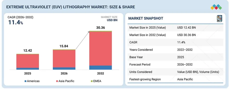
The global extreme ultraviolet (EUV) lithography market is expected to grow from USD 15.84 billion in 2026 to USD 30.36 billion by 2032, at a CAGR of 11.4%. The rapid advancements in consumer electronics, including smartphones, wearables, tablets, and gaming devices, are driving sustained demand for advanced semiconductor chips that offer higher performance, compact designs, and improved energy efficiency. To support faster processing, enhanced graphics, and longer battery life, manufacturers increasingly rely on EUV lithography to enable smaller transistors and higher transistor density.
Scope of the Report
Years Considered for the Study
2021-2032
Base Year
2024
Forecast Period
2025-2032
Units Considered
Value (USD Billion)
Segments
By Component, System Type, End User and Region
Regions covered
North America, Europe, APAC, RoW
The shift toward next-generation technologies, including foldable displays, augmented reality, and virtual reality, is further increasing chip complexity and reinforcing the need for high-precision EUV-based manufacturing. As performance and miniaturization requirements continue to rise across consumer electronics and autonomous applications, EUV lithography is becoming a critical enabler for producing reliable, high-performance integrated circuits at advanced nodes.
"Light sources to exhibit highest CAGR from 2026 to 2032."
Light sources are expected to witness the highest CAGR in the extreme ultraviolet (EUV) lithography market due to their direct impact on system productivity, throughput, and cost efficiency at advanced semiconductor nodes. Continuous demand for higher wafer throughput is driving the need for increased EUV source power, improved stability, and longer uptime, prompting frequent upgrades and replacements of existing light source modules. In addition, the transition toward more advanced process nodes and the gradual shift to next-generation EUV platforms are increasing performance requirements for light sources, accelerating R&D investments and adoption. The high technical complexity, limited supplier base, and strong focus on productivity-driven enhancements further support faster revenue growth for this component compared to other EUV system elements.
"Logic chips held largest share of extreme ultraviolet (EUV) lithography market in 2025."
Logic chips held the largest market share in the application segment of the extreme ultraviolet (EUV) lithography market in 2025, driven by early and widespread adoption of EUV at advanced process nodes. Leading-edge logic devices at 7 nm, 5 nm, and 3 nm require extremely fine patterning, tight overlay control, and high transistor density, all of which are more efficiently achieved using EUV compared with multi-patterning DUV techniques. The rapid growth of applications such as artificial intelligence, high-performance computing, data centers, and advanced automotive electronics is driving strong demand for high-performance logic chips, accelerating EUV tool utilization and capacity expansion. In contrast, memory manufacturers have adopted EUV more selectively, focusing on specific layers, which further reinforces the dominance of logic chips in overall extreme ultraviolet (EUV) lithography demand.
"Asia Pacific to be fastest-growing regional market for EUV lithography from 2026 to 2032."
Asia Pacific is expected to register the highest CAGR during the forecast period, driven by its strong concentration of leading semiconductor foundries and integrated device manufacturers (IDMs), as well as continuous investments in advanced-node manufacturing. The region's dominance is supported by large-scale capacity expansions at 5 nm, 3 nm, and sub-3 nm nodes, rising demand for logic chips used in AI, high-performance computing, and advanced consumer electronics, and a mature semiconductor supply chain that enables rapid EUV adoption. In addition, sustained capital expenditure, aggressive technology roadmaps, and government-backed initiatives to strengthen domestic semiconductor capabilities are accelerating EUV tool installations. These factors collectively position Asia Pacific as the primary demand center and growth engine for the global extreme ultraviolet (EUV) lithography market.
Breakdown of Primaries
Various executives from key organizations operating in the extreme ultraviolet (EUV) lithography market were interviewed in-depth, including CEOs, marketing directors, and innovation and technology directors.
By Company Type: Tier 1-30%, Tier 2-50%, and Tier 3-20%
By Designation: C-level Executives-25%, Directors-35%, and Others-40%
By Region: Asia Pacific-40%, Americas-25%, and EMEA- 35%
The extreme ultraviolet (EUV) lithography market is dominated by ASML (Netherlands) as the sole manufacturer of EUV lithography products, as well as by component manufacturers such as TRUMPF (Germany), Ushio Inc. (Japan), Energetiq (US), Zeiss Group (Germany), NTT Advanced Technology Corporation (Japan), Rigaku Holdings Corporation (Japan), Edmund Optics Inc. (US), AGC Inc. (Japan), Tekscend Photomask (Japan), Lasertec Corporation (Japan), HOYA Corporation (Japan), NuFlare Technology, Inc. (Japan), KLA Corporation (US), ADVANTEST CORPORATION (Japan), SUSS MicroTec SE (Germany), Applied Materials, Inc. (US), Park Systems (South Korea), Imagine Optic (France), MKS Inc. (US), Taiwan Semiconductor Manufacturing Company Limited (TSMC) (Taiwan), Intel Corporation (US), Samsung (South Korea), SK HYNIX INC. (South Korea), and Micron Technology (US). The study includes an in-depth competitive analysis of these key players in the extreme ultraviolet (EUV) lithography market, with their company profiles, recent developments, and key market strategies.
Study Coverage
The report segments the extreme ultraviolet (EUV) lithography market and forecasts its components, system types, end users, applications, and regions. The report also discusses the drivers, restraints, opportunities, and challenges pertaining to the market. It provides a detailed view of the market across three main regions-Americas, Asia Pacific, and EMEA. The report includes a value chain analysis of the key players and their competitive analysis of the EUV lithography ecosystem.
Key Benefits of Buying the Report
Analysis of key drivers (surging deployment of EUV lithography across leading-edge foundry nodes), restraints (high upfront capital investment), opportunities (increasing investments in advanced EUV lithography and semiconductor devices), and challenges (competition from alternative lithography techniques) influencing the growth of the extreme ultraviolet (EUV) lithography market
Products/Solution/Service Development/Innovation: Detailed insights into upcoming components, technologies, research, and development activities in the extreme ultraviolet (EUV) lithography market
Market Development: Comprehensive information about lucrative markets-the report analyzes the extreme ultraviolet (EUV) lithography market across varied regions
Market Diversification: Exhaustive information about new EUV lithography in untapped geographies, recent developments, and investments in the extreme ultraviolet (EUV) lithography market
Competitive Assessment: In-depth assessment of market shares and growth strategies, and offerings of leading players offering components of EUV lithography, such as KLA Corporation (US), ZEISS Group (Germany), TRUMPF (Germany), AGC Inc. (Japan), and Lasertec Corporation (Japan)
TABLE OF CONTENTS
1 INTRODUCTION
1.1 STUDY OBJECTIVES
1.2 MARKET DEFINITION
1.3 STUDY SCOPE
1.3.1 MARKETS COVERED AND REGIONAL SCOPE
1.3.2 INCLUSIONS AND EXCLUSIONS
1.3.3 YEARS CONSIDERED
1.4 CURRENCY CONSIDERED
1.5 UNIT CONSIDERED
1.6 LIMITATIONS
1.7 STAKEHOLDERS
1.8 SUMMARY OF CHANGES
2 EXECUTIVE SUMMARY
2.1 MARKET HIGHLIGHTS AND KEY INSIGHTS
2.2 KEY MARKET PARTICIPANTS: MAPPING OF STRATEGIC DEVELOPMENTS
2.3 DISRUPTIVE TRENDS IN EXTREME ULTRAVIOLET (EUV) LITHOGRAPHY MARKET
2.4 HIGH-GROWTH SEGMENTS
2.5 REGIONAL SNAPSHOT: MARKET SIZE, GROWTH RATE, AND FORECAST
3 PREMIUM INSIGHTS
3.1 ATTRACTIVE OPPORTUNITIES FOR PLAYERS IN EXTREME ULTRAVIOLET (EUV) LITHOGRAPHY MARKET
3.2 EXTREME ULTRAVIOLET (EUV) LITHOGRAPHY MARKET, BY END USER
3.3 EXTREME ULTRAVIOLET (EUV) LITHOGRAPHY MARKET, BY APPLICATION
3.4 EXTREME ULTRAVIOLET (EUV) LITHOGRAPHY MARKET, BY REGION
4 MARKET OVERVIEW
4.1 INTRODUCTION
4.2 MARKET DYNAMICS
4.2.1 DRIVERS
4.2.1.1 Surging deployment of EUV lithography across leading-edge foundry nodes
4.2.1.2 Elevating use of AI accelerators and deep learning processors in HPC systems
4.2.1.3 Increasing complexity of integrated circuits
4.2.1.4 Rapid advancements in consumer electronics
4.2.2 RESTRAINTS
4.2.2.1 High upfront capital investment
4.2.2.2 Requirement for advanced infrastructure and skilled workforce
4.2.3 OPPORTUNITIES
4.2.3.1 Increasing investments in advanced EUV lithography and semiconductor devices
4.2.3.2 Emerging applications of EUV lithography
4.2.3.3 Advancements in memory modules and chips
4.2.3.4 Integration of EUV lithography into advanced display manufacturing
4.2.3.5 Application of advanced patterning technologies in photonics and optics production
4.2.3.6 Commercialization of High-NA EUV lithography
4.2.4 CHALLENGES
4.2.4.1 Competition from alternative lithography techniques
4.2.4.2 Difficulty in sustaining high source power and productivity
4.2.4.3 Detecting and addressing mask defects and yield-related challenges
5 INDUSTRY TRENDS
5.1 INTRODUCTION
5.2 PORTER'S FIVE FORCES ANALYSIS
5.2.1 INTENSITY OF COMPETITIVE RIVALRY
5.2.2 THREAT OF NEW ENTRANTS
5.2.3 THREAT OF SUBSTITUTES
5.2.4 BARGAINING POWER OF BUYERS
5.2.5 BARGAINING POWER OF SUPPLIERS
5.3 MACROECONOMIC OUTLOOK
5.3.1 INTRODUCTION
5.3.2 GDP TRENDS AND FORECAST
5.3.3 TRENDS IN FOUNDRIES
5.3.4 TRENDS IN INTEGRATED DEVICE MANUFACTURERS (IDMS)
5.4 VALUE CHAIN ANALYSIS
5.4.1 R&D ENGINEERS
5.4.2 RAW MATERIAL PROVIDERS AND COMPONENT MANUFACTURERS
5.4.3 SYSTEM INTEGRATORS AND MANUFACTURERS
5.4.4 MARKETING & SALES SERVICES PROVIDERS
5.4.5 END USERS
5.5 ECOSYSTEM ANALYSIS
5.6 PRICING ANALYSIS
5.6.1 AVERAGE SELLING PRICE TREND OF EUV LITHOGRAPHY SYSTEM TYPES, BY KEY PLAYER, 2021-2025
5.6.2 AVERAGE SELLING PRICE TREND OF EUV LITHOGRAPHY SYSTEM, BY REGION, 2021-2025
5.7 TRADE ANALYSIS
5.7.1 IMPORT SCENARIO (HS CODE 8442)
5.7.2 EXPORT SCENARIO (HS CODE 8442)
5.8 KEY CONFERENCES AND EVENTS, 2026-2027
5.9 TRENDS/DISRUPTIONS IMPACTING CUSTOMER BUSINESS