


세계의 3D 스태킹 시장은 2024년 18억 달러에 달했고, CAGR 21.1%로 성장하여 2034년까지 118억 달러에 이를 것으로 예측되고 있습니다.
이 놀라운 성장은 소비자 전자 제품, 고성능 컴퓨팅 시스템 및 첨단 반도체 기술에 대한 수요 증가로 인한 것입니다. 인공지능(AI), 머신러닝, 사물인터넷(IoT) 등의 데이터 집약적인 용도이 계속 확대되고 있는 가운데, 데이터 처리의 고속화, 효율의 향상, 전력 관리의 개선에 대한 요구는 그 어느 때보다도 중요해지고 있습니다. 3D 스태킹 기술은 로직, 메모리, 인터커넥트와 같은 여러 기능 레이어를 컴팩트한 실적에 통합함으로써 디바이스 제조업체가 이러한 진화하는 요구를 충족할 수 있도록 하는 것으로, 반도체 혁신의 미래를 담당하는 것으로 점점 주목받고 있습니다. 전자 산업이 성능을 희생하지 않고 소형화를 추진하는 동안, 3D 스태킹은 높은 처리량, 낮은 대기 시간 및 우수한 열 관리를 제공하는 이상적인 경로를 제공합니다. 스마트폰 및 웨어러블부터 데이터센터 프로세서, 자율주행차까지 이 기술의 적용 범위가 급속히 확대되고 있습니다. 칩렛 기반 설계와 이종 집적의 채택은 이 시장의 기세를 더욱 가속화하고 업계에 관계없이 특정 이용 사례에 맞게 솔루션을 사용자 정의할 수 있는 유연성을 제공합니다.
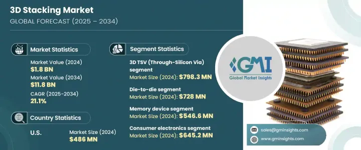
3D 스태킹 기술은 3D 하이브리드 본딩, 3D 관통 전극(TSV), 모놀리식 3D 집적 등 상호 연결 방식에 따라 분류됩니다. 이 중 3D TSV 분야는 2024년 7억 9,830만 달러를 창출했습니다. 이 분야는 데이터센터, HPC 플랫폼 및 자율 시스템의 성능 요구 사항을 지원하는 고속, 낮은 대기 시간 메모리 인터페이스에 대한 수요가 증가함에 따라 강력한 성장을 이루고 있습니다. 또한 5G 네트워크의 배포와 스마트 디바이스의 보급으로 엄청난 양의 실시간 데이터 처리를 관리할 수 있는 에너지 효율적인 컴팩트한 칩 아키텍처의 요구도 높아지고 있습니다.
| 시장 범위 | |
|---|---|
| 시작 연도 | 2024년 |
| 예측 연도 | 2025-2034년 |
| 시작 금액 | 18억 달러 |
| 예측 금액 | 118억 달러 |
| CAGR | 21.1% |
이 시장은 또한 다이 투 웨이퍼, 웨이퍼 투 웨이퍼, 다이 투 다이, 칩 투 칩, 칩 투 웨이퍼 등의 상호 접속 기술별로 구분됩니다. 2024년 다이 투 다이 시장 규모는 7억 2,800만 달러였습니다. 이 기술은 다이 간 원활한 통신이 필요한 멀티칩 모듈과 칩셋 기반 아키텍처에 특히 중요합니다. AI 가속기, 클라우드 인프라, HPC 프로세서의 진보에 중요한 역할을 하여 설계 유연성 향상, 에너지 절약 강화, 확장성 향상을 실현합니다.
미국의 3D 스태킹 시장은 2024년에 4억 8,600만 달러를 창출하였습니다. 미국의 반도체 기업은 차세대 컴퓨팅에서 성능, 에너지 효율 및 확장성의 한계를 넓히기 위해 칩렛 아키텍처 및 TSV 기반 설계 개발에 자원을 쏟고 있습니다.
세계 3D 스태킹 시장의 주요 기업은 AMD, ASE Technology Holding, Amkor Technology, Broadcom, IBM, Intel, Graphcore, JCET Group, Marvell Technology, Micron Technology, Kioxia, NVIDIA, OmniVision Technologies, SK Hynix, Sony Semi Electronics, SPIL, Western Digital, Xilinx 등이 있습니다. 이러한 기업은 AI, 데이터센터, 고성능 컴퓨팅 시장에서의 수요 증가에 대응하기 위해, 칩 적층과 상호 접속 수법의 혁신을 가속화하고 있습니다.
The Global 3D Stacking Market was valued at USD 1.8 billion in 2024 and is expected to grow at a CAGR of 21.1% to reach USD 11.8 billion by 2034. This remarkable growth is largely attributed to the rising demand for consumer electronics, high-performance computing systems, and advanced semiconductor technologies. As data-intensive applications such as artificial intelligence (AI), machine learning, and the Internet of Things (IoT) continue to scale, the need for faster data processing, enhanced efficiency, and improved power management becomes more critical than ever. 3D stacking technology is increasingly seen as the future of semiconductor innovation, enabling device manufacturers to meet these evolving needs by integrating multiple functional layers-such as logic, memory, and interconnects-within a compact footprint. As the electronics industry pushes toward miniaturization without compromising performance, 3D stacking provides an ideal pathway to achieve higher throughput, lower latency, and superior thermal management. From smartphones and wearables to data center processors and autonomous vehicles, the scope of applications for this technology is rapidly expanding. The adoption of chiplet-based designs and heterogeneous integration further drives this market's momentum, offering the flexibility to customize solutions for specific use cases across industries.

3D stacking technology is classified based on interconnection methods, including 3D hybrid bonding, 3D Through-Silicon Via (TSV), and monolithic 3D integration. Among these, the 3D TSV segment generated USD 798.3 million in 2024. This segment is experiencing robust growth due to rising demand for high-speed, low-latency memory interfaces that support the performance requirements of data centers, HPC platforms, and autonomous systems. The rollout of 5G networks and the proliferation of smart devices are also intensifying the need for energy-efficient and compact chip architectures that can manage vast volumes of real-time data processing.
| Market Scope | |
|---|---|
| Start Year | 2024 |
| Forecast Year | 2025-2034 |
| Start Value | $1.8 Billion |
| Forecast Value | $11.8 Billion |
| CAGR | 21.1% |
The market is further segmented by interconnect technology, including die-to-wafer, wafer-to-wafer, die-to-die, chip-to-chip, and chip-to-wafer techniques. The die-to-die segment was valued at USD 728 million in 2024. This method is especially vital for multi-chip modules and chipset-based architectures that require seamless communication between dies. It plays a key role in advancing AI accelerators, cloud infrastructure, and HPC processors, offering greater design flexibility, enhanced energy savings, and improved scalability.
United States 3D Stacking Market generated USD 486 million in 2024. The region is witnessing substantial growth owing to increased investments in AI applications, advanced data center operations, and HPC infrastructure. US-based semiconductor firms are channeling resources into developing chiplet architectures and TSV-based designs to push the boundaries of performance, energy efficiency, and scalability in next-gen computing.
Key players in the Global 3D Stacking Market include AMD, ASE Technology Holding, Amkor Technology, Broadcom, IBM, Intel, Graphcore, JCET Group, Marvell Technology, Micron Technology, Kioxia, NVIDIA, OmniVision Technologies, SK Hynix, Sony Semiconductor Solutions, Samsung Electronics, SPIL, Western Digital, and Xilinx. These companies are accelerating innovations in chip stacking and interconnect methodologies to address the growing demand from AI, data center, and high-performance computing markets. Through focused R&D and strategic investments, they aim to deliver future-ready semiconductor solutions that combine power efficiency, superior performance, and architectural flexibility.