


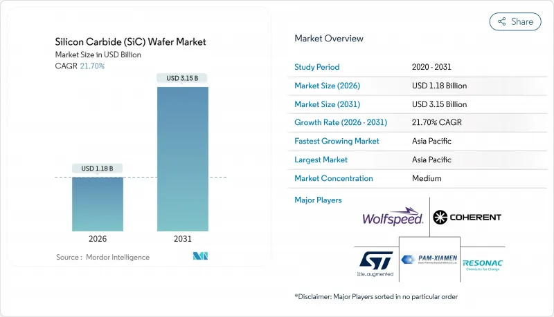
실리콘 카바이드(SiC) 웨이퍼 시장 규모는 2026년 11억 8,000만 달러로 평가되었고, 2025년 9억 7,000만 달러에서 성장할 것으로 보이며, 2031년에는 31억 5,000만 달러에 이를 것으로 예측됩니다. 2026-2031년에 걸쳐 CAGR 21.7%로 성장할 전망입니다.

자동차 산업의 800V 차량 플랫폼 전환, 산업용 전력 전자 장치의 와이드밴드갭 채택 확대, 신규 생산라인 구축을 지원하는 정부 인센티브가 성장 궤도를 뒷받침하고 있습니다. 지속적으로 개선되는 결정 성장 수율, 8인치 기판의 공급 확대, 효율적인 고속 충전 인프라에 대한 수요 증가는 확장을 더욱 견고히 합니다. 아시아태평양 지역은 2024년 최대 지역 점유율을 기록했으며, 수직 통합형 생태계가 상류 및 하류 투자를 지속적으로 유치하고 있습니다. 자본 집약도는 여전히 주요 경쟁 필터로 작용하지만, 결함 감소, 웨이퍼 스케일링, 내부 공급망 관리 기술을 확보한 기업들은 고온 및 고주파 작동 환경에서 기존 실리콘을 능가하는 실리콘 카바이드 웨이퍼 시장의 다음 수요 물결을 선점할 수 있는 위치에 있습니다.
테슬라 모델 S 플레이드, 현대 아이오닉 5, 기아 EV6 등 모델을 통해 자동차 제조사들은 대규모 800V 시스템 채택을 입증했습니다. 이러한 고전압 아키텍처는 충전 시간을 20분 이하로 단축시켰으나, 높은 열적 및 전기적 스트레스를 견딜 수 있는 파워 MOSFET을 요구했습니다. 실리콘 카바이드는 실리콘 대비 10배 높은 임계 전기장과 3배 높은 열전도율로 이러한 기준을 충족하여, 트랙션 인버터 및 온보드 충전기 수요를 확대시켰다. 럭셔리 및 프리미엄 부문이 이 기술을 먼저 도입했으나, 웨이퍼 비용 하락과 공급망 성숙화로 주류 전기차 플랫폼으로의 확산이 가속화되며 실리콘 카바이드 웨이퍼 시장은 차세대 모빌리티의 핵심 기반 기술로 자리매김하고 있습니다.
충전 네트워크 운영사들은 350kW 충전소에서 변환 손실을 최소화하기 위해 실리콘 카바이드를 선택했습니다. 일렉트리파이 아메리카의 플래그십 사이트는 실리콘 대비 더 높은 전력 밀도와 낮은 발열을 달성하기 위해 SiC 기반 정류기와 DC-DC 모듈을 통합했습니다. 유럽 고속도로 충전망 업체 IONITY도 유사한 방식을 채택하며, 자동차 제조사들이 800V 플랫폼을 채택하도록 유도하는 공급-수요 플라이휠을 형성했습니다. 차량, 충전기, 전력망 연계 장비로 확장된 이 생태계는 웨이퍼 수요를 증가시키는 동시에 에너지 효율성 향상으로 네트워크 운영사의 총소유비용을 절감합니다.
200mm 부울의 결정 성장 사이클은 종종 200시간을 초과했으며 150mm에 비해 더 높은 결함 밀도를 보였기 때문에 자동차 등급 기판의 공급이 제한되었습니다. 수율 저하로 웨이퍼 평균판매가격(ASP)이 상승하고 대형 직경으로의 설계 전환이 지연되었습니다. 제조업체들은 격차를 해소하기 위해 첨단 현장 모니터링 및 시드 결정체 최적화에 투자했으나, 특히 엄격한 품질 기준을 요구하는 자동차 제조업체를 중심으로 단기적 공급 부족이 계속되어 실리콘 카바이드 웨이퍼 시장 출하량 성장을 제한하고 있습니다.
2025년 실리콘 카바이드 웨이퍼 시장에서는 6인치 웨이퍼가 53.75%의 점유율을 차지했습니다. 웨이퍼당 디바이스수와 다이당 감가상각비가 이 기존 지름을 양산기준으로 자리매김하고 있습니다. 그러나, 8인치 웨이퍼는 2031년까지 28.6%의 연평균 복합 성장률(CAGR)로 확대될 것으로 예측되고 있으며, 트랙션 인버터 및 PV 인버터에서의 암페어당 비용 우위성을 뒷받침하고 있습니다. 200mm 결정용 고온 PVT 퍼니스와 같은 장비 투자 비용은 1,500만-2,000만 달러로 6인치용 800만-1,200만 달러에 비해 훨씬 높습니다. 그러나 8인치 웨이퍼 당 다이 생산량은 최대 2.2배에 이르며 수율 향상에 따라 비용 곡선이 단축됩니다. 스케일 메리트가 나타날수록 8인치 기판 실리콘 카바이드 웨이퍼 시장 규모는 점점 더 큰 수익원이 될 전망입니다.
2024년 수율률은 6인치 대비 15-20% 뒤처졌으나, 핫존 설계 최적화 및 결함 감소 분석 기술에 대한 투자가 격차를 좁혔습니다. 자동차 및 재생에너지 통합업체들은 200mm 다이에 대한 인증 프로그램을 시작했으며, 이는 대량 공급이 안정화되면 더 넓은 수용이 이루어질 것임을 시사합니다. 4인치 미만 포맷은 연구개발이 고전압 자동차 또는 그리드 모듈로 이동함에 따라 계속 감소한 반면, 12인치 이상의 프로토타입은 학계에 국한되었습니다. 따라서 8인치로의 성공적인 규모 확대는 실리콘 카바이드 웨이퍼 시장의 중대한 전환점으로 자리매김하고 있습니다.
2025년 N형 전도성 웨이퍼는 실리콘 카바이드 웨이퍼 시장 점유율의 68.12%를 차지했습니다. 낮은 저항률과 안정적인 도판트 프로파일로 인해 파워 MOSFET, 다이오드, 쇼트키 소자 제조에 필수적이었습니다. 반절연 기판은 역사적으로 틈새 시장이었으나, 5G 기지국, 레이더, 위성 페이로드에서의 RF 및 마이크로파 채택으로 2031년까지 연평균 23.6% 성장률을 기록할 전망입니다. 네트워크 고밀도화와 방위 전자장비가 기가헤르츠 주파수에서 기생 커패시턴스를 제한하기 위해 순수하고 전기적으로 절연된 격자를 요구함에 따라, 반절연 소재에 할당된 실리콘 카바이드 웨이퍼 시장 규모는 확대될 것입니다.
제조사들은 더 큰 직경에서 저항률 균일성을 높이기 위해 성장 후 어닐링 및 보상 도핑 기술을 지속적으로 개선하고 있습니다. 항공우주 및 통신 기업들은 우수한 열 관리 성능을 제공하는 GaN-on-SiC HEMT용 반절연 웨이퍼를 선호합니다. 그 결과, 높은 열전도도, 전기적 절연성 및 우수한 RF 성능을 보장하는 기판을 중시하는 경쟁 환경이 점차 확대되고 있습니다. 이러한 추세는 차세대 소자 아키텍처 진화에서 반절연 실리콘 카바이드의 핵심적 역할을 부각시킵니다.
실리콘 카바이드(SiC) 웨이퍼 시장은 웨이퍼 직경(4인치 미만, 4인치 이상), 도전 유형(N형 전도성, 반절연), 용도별(파워 일렉트로닉스, RF 디바이스 등), 최종 이용 산업별(자동차 및 전기자동차, 재생에너지 및 축전 등), 결정 성장 기술별(PVT, CVD 등), 지역별로 분류됩니다. 시장 예측은 금액 기준(달러)으로 제공됩니다.
북미는 리쇼어링 인센티브와 깊이 있는 전기차 생태계에 힘입어 2위를 차지했습니다. Wolfspeed의 모호크 밸리 공장은 200mm 웨이퍼 생산을 확대했으며, 테슬라가 대규모 SiC 트랙션 인버터를 검증하면서 지역 공급 계약이 촉진되었습니다. 온세미는 체코에 최대 20억 달러를 투자해 SiC 생산의 전 과정을 구축하기로 약속했으며, 이는 유럽 자동차 OEM에 선택권을 제공하면서도 미국의 기술 리더십을 유지하는 방안입니다. 로옴과 SK 실트론의 프리미엄 기판 생산을 통해 기술 리더십을 유지함으로써 가격 하락 압박에도 불구하고 높은 평균판매가격(ASP)을 유지하고 있습니다.
북미는 리쇼어링 우대책과 충실한 EV 에코시스템을 배경으로 2위를 유지했습니다. 울프 스피드사의 모호크 밸리 공장에서는 200mm 웨이퍼의 양산이 개시되어 테슬라사에 의한 대규모 SiC 트랙션 인버터의 검증이 지역공급 계약을 촉진했습니다. 온세미컨덕터는 체코 공화국에서 SiC의 엔드 투 엔드 생산 체제 구축에 최대 20억 달러를 투자하고 유럽 자동차 제조업체에 옵션을 제공하면서 미국의 기술적 우위성을 유지하고 있습니다.
유럽은 그린딜에 의한 전동화 정책과 견고한 자동차 기반을 배경으로 진전했습니다. 인피니언은 오스트리아와 독일에서 웨이퍼 생산을 확대해 포르쉐 및 아우디의 800V 플랫폼에 대응. 최저 비용보다 품질과 신뢰성을 강조했습니다. ST 마이크로 일렉트로닉스는 카타니아 공장을 확장하고 EU의 반도체 자급 목표에 따른 지역 공급망의 기반을 확립. 실리콘 카바이드 웨이퍼 시장은 가격 민감도가 계속되고 있지만 유럽 구매자는 자동차 등급 추적성과 엄격한 결함 사양을 중시했습니다.
The silicon carbide wafer market size in 2026 is estimated at USD 1.18 billion, growing from 2025 value of USD 0.97 billion with 2031 projections showing USD 3.15 billion, growing at 21.7% CAGR over 2026-2031.
The growth trajectory is supported by the automotive industry's migration to 800 V vehicle platforms, wide-band-gap adoption in industrial power electronics, and government incentives that underwrite new fabrication lines. Steadily improving crystal-growth yields, wider availability of 8-inch substrates, and rising demand for efficient fast-charging infrastructure further underpin expansion. Asia-Pacific held the largest regional share in 2024, and its vertically integrated ecosystem continues to attract upstream and downstream investments. Capital intensity remains a key competitive filter, yet companies that master defect reduction, wafer scaling, and internal supply chains are positioned to capture the next wave of demand as the silicon carbide wafer market outperforms conventional silicon in high-temperature and high-frequency operating environments.
Automakers demonstrated large-scale 800 V system adoption through models such as Tesla's Model S Plaid, Hyundai's IONIQ 5, and Kia's EV6. These high-voltage architectures reduced charging times well below 20 minutes yet demanded power MOSFETs capable of withstanding elevated thermal and electrical stress. Silicon carbide meets these thresholds due to a ten-fold higher critical electric field and three-fold higher thermal conductivity than silicon, which magnifies demand in traction inverters and onboard chargers. Luxury and premium segments adopted the technology first, but falling wafer costs and maturing supply chains now accelerate diffusion into mainstream EV platforms, reinforcing the silicon carbide wafer market as an essential enabler of next-generation mobility.
Charging network operators selected silicon carbide to minimise conversion losses in 350 kW stations. Electrify America's flagship sites integrated SiC-based rectifiers and DC-DC modules, achieving higher power density and lower heat dissipation compared with silicon. European corridor provider IONITY followed a similar path, creating a supply-demand flywheel that encourages automakers to embrace 800 V platforms. The resulting ecosystem, spanning vehicles, chargers, and grid-interfacing equipment, ramps up wafer volumes while compressing total ownership cost for network operators through energy-efficiency savings.
Crystal-growth cycles for 200 mm boules often exceeded 200 hours and yielded higher defect densities than 150 mm equivalents, constraining the supply of automotive-grade substrates. Yield penalties elevated wafer ASPs and delayed design transitions to larger diameters. Fabricators invested in advanced in-situ monitoring and seed-crystal optimisation to close the gap, yet near-term shortages continue to cap silicon carbide wafer market shipment growth, especially for carmakers that require stringent quality thresholds.
Other drivers and restraints analyzed in the detailed report include:
For complete list of drivers and restraints, kindly check the Table Of Contents.
The silicon carbide wafer market recorded 6-inch substrates at 53.75% share in 2025. Device counts per wafer and depreciation per die positioned this legacy diameter as the volume benchmark. However, 8-inch substrates are forecast to expand at a 28.6% CAGR through 2031, underscoring the cost-per-ampere advantage for traction inverters and PV inverters. Equipment investments remain high-PVT furnaces for 200 mm crystals cost USD 15-20 million versus USD 8-12 million for 6-inch. Nonetheless, each 8-inch wafer can deliver up to a 2.2-fold increase in die output, tightening the cost curve as yields improve. The silicon carbide wafer market size for 8-inch substrates is projected to command an increasingly large revenue pool as scale economies kick in.
Although yield rates lagged 6-inch equivalents by 15-20% in 2024, investment in hot-zone design optimisation and defect-reduction analytics narrowed the gap. Automotive and renewable energy integrators began qualification programs for 200 mm die, signalling broader acceptance once volume supply stabilises. less than 4-inch formats continued to decline as R&D moves toward high-voltage automotive or grid modules, while above 12-inch prototypes remained confined to academia. Successful scale-up to 8-inch thus stands as the pivotal inflection point for the silicon carbide wafer market.
N-type conductive wafers accounted for 68.12% of the silicon carbide wafer market share in 2025. Their low resistivity and stable dopant profiles made them indispensable for power MOSFETs, diodes, and Schottky devices. Semi-insulating substrates, although historically niche, are poised for 23.6% CAGR growth to 2031, driven by RF and microwave adoption in 5G base stations, radar, and satellite payloads. The silicon carbide wafer market size allocated to semi-insulating material is set to swell as network densification and defense electronics demand pure, electrically isolated lattices to limit parasitic capacitance at gigahertz frequencies.
Producers continue to refine post-growth annealing and compensation-doping techniques to lift resistivity uniformity across larger diameters. Aerospace and telecommunications firms favour semi-insulating wafers for GaN-on-SiC HEMTs that deliver superior thermal handling. As a result, the competitive landscape increasingly values substrates that ensure high thermal conductivity, electrical isolation, and superior RF performance. This trend highlights semi-insulating silicon carbide as a pivotal player in the evolution of next-generation device architectures.
Silicon Carbide (SiC) Wafer Market is Segmented by Wafer Diameter (less Than 4 Inch, and More), Conductivity Type (N-Type Conductive and Semi-Insulating), Application (Power Electronics, RF Devices, and More), End-Use Industry (Automotive and Electric Vehicles, Renewable Energy and Storage, and More), Crystal-Growth Technology (PVT, CVD, and More), and Geography. The Market Forecasts are Provided in Terms of Value (USD).
North America ranked second, bolstered by reshoring incentives and a deep EV ecosystem. Wolfspeed's Mohawk Valley fab ramped 200 mm wafers, and Tesla validated large-scale SiC traction inverters, spurring regional supply agreements. OnSemi committed up to USD 2 billion to establish end-to-end SiC production in the Czech Republic, providing optionality for European auto OEMs while retaining US technology leadership.chnology leadership through premium substrate production at ROHM and SK Siltron, preserving high ASPs despite down-price pressure.
North America ranked second, bolstered by reshoring incentives and a deep EV ecosystem. Wolfspeed's Mohawk Valley fab ramped 200 mm wafers, and Tesla validated large-scale SiC traction inverters, spurring regional supply agreements. OnSemi committed up to USD2 billion to establish end-to-end SiC production in the Czech Republic, providing optionality for European auto OEMs while retaining US technology leadership.
Europe advanced on the back of Green Deal electrification policies and a strong automotive base. Infineon expanded wafer output in Austria and Germany to serve Porsche and Audi 800 V platforms, emphasising quality and reliability over lowest cost. STMicroelectronics scaled its Catania site, anchoring a local supply chain that aligned with EU semiconductor sovereignty goals. Although the silicon carbide wafer market remained price sensitive, European buyers valued automotive-grade traceability and tight defect specifications.