


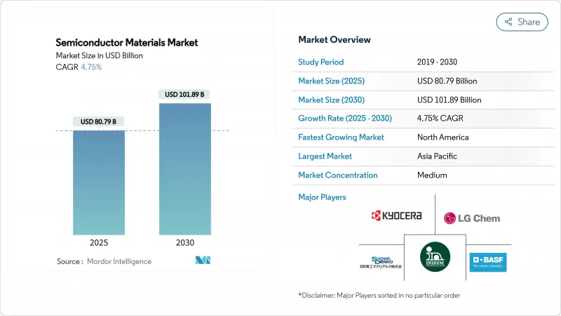
반도체 재료 시장 규모는 2025년에 807억 9,000만 달러로 평가되었고, 2030년에 1,018억 9,000만 달러에 이를 것으로 `예측되며, 예측 기간 동안 CAGR은 4.75%를 나타낼 전망입니다.

인공지능(AI) 최적화 아키텍처와 자동차 전동화가 지속되면서 기존 실리콘이 물리적 한계에 근접함에 따라 소재 요구사항이 재편되고 있습니다. 첨단 패키징 소재 시장은 11.8%의 연평균 복합 성장률(CAGR)로 가속화되고 있는데, 이는 칩렛 설계와 3D 적층 아키텍처가 새로운 상호연결 및 열 관리 솔루션을 필요로 하기 때문입니다. 2024년 기준 제조 소재가 여전히 63%의 매출 점유율로 우위를 점하고 있으나, 가치 창출은 패키징 혁신이 시스템 성능을 점점 더 좌우하는 하류 공정으로 이동 중입니다. 전기차용 광대역갭 전력 소자로의 전환과 북미 및 유럽의 국내 소재 공급망 유인을 위한 전략적 리쇼어링 프로그램도 수요를 부양하고 있습니다. 핵심 화학물질 관련 지정학적 긴장(특히 2019년 일본의 불화수소 수출 제한)은 다각화된 조달 전략의 중요성을 부각시켰습니다.
2027년까지 300mm 팹 장비를 위해 배정된 4,000억 달러는 반도체 역사상 가장 큰 규모의 생산 능력 확장을 의미합니다. 텍사스 인스트루먼트(TI)만 해도 미국 내 7개 팹에 600억 달러를 투자하기로 했으며, 마이크론은 국내 메모리 시설에 2,000억 달러를 계획 중입니다. 각 첨단 팹은 이전 세대보다 웨이퍼당 특수 화학 물질 소비량이 40% 증가하여, 공급업체들이 여러 지역에서 초고순도 생산을 확대해야 하는 압박이 가중되고 있습니다.
AI 가속기는 전례 없는 대역폭과 열적 한계를 요구하여 패키지당 재료비를 기존 프로세서 대비 3배로 증가시킵니다. HBM 스택은 실리콘 관통 전극(TSV) 구리 필러와 초박형 다이 부착 필름에 의존하며, 이는 은 함량이 높은 제형을 필요로 합니다. 후지필름은 2030년까지 반도체 소재 매출 5,000억 엔 달성을 목표로 하고 있으며, 이는 주로 AI 중심 노드에 맞춤화된 EUV 포토레지스트에서 발생할 전망입니다. 자동차 부문에서는 LG화학의 SiC 파워 모듈용 고성능 은 페이스트가 AI 기반 모빌리티가 온도와 전압 요구 사항을 동시에 높이는 방식을 보여줍니다.
반도체 패키징 소재 부문은 2023년 15.5% 하락한 후 2024년 반등하며, 스마트폰과 PC 수요 둔화가 화학 수요에 빠르게 파급되는 양상을 보여줍니다. 분기 내 최대 30%에 달하는 재고 변동은 대량 생산 소비자 제품 라인에 집중된 공급업체에 부담을 줍니다. 자동차, 산업 및 인프라 분야로의 다각화가 이러한 변동성을 완화하고 있지만 완전히 제거하지는 못하고 있습니다. AI 강화형 소비자 기기의 등장은 주기적 변동폭을 낮출 수 있으나, 매출 성장의 주요 동력이 단위 판매 증가에서 부품 원가 상승으로 대체되면서 예측 복잡성을 새롭게 도입할 수 있습니다.
2024년 제조 재료 부문은 웨이퍼당 수백 단계의 식각, 증착, 평탄화 공정을 반영하여 전체 매출의 63%를 차지했습니다. 습식 화학물질, 전자 가스, CMP 소모품이 가장 큰 비용 항목을 구성합니다. 가치 기준으로 이 반도체 재료 시장 부문은 2024년 500억 달러 이상에 달했습니다. 고급 패키징은 현재 규모는 작지만, 칩릿 분할이 금속화 밀도와 열 인터페이스 성능을 유기 라미네이트의 한계를 넘어 확장시키면서 9.2%의 연평균 성장률(CAGR)로 성장하고 있습니다. 따라서 반도체 재료 시장은 패키징 원자재의 11.8% CAGR 성장에 힘입어 다중 다이 아키텍처를 위해 설계된 기판, 언더필, 몰드 컴파운드로 기울고 있습니다.
이러한 전환은 산업 내 권력 역학도 재편하고 있습니다. 제조 공급업체는 규모의 경제를 누리지만 성장 곡선은 완만해지는 반면, 패키징 혁신 기업들은 장기적 탄력성이 높은 설계 도입(design-in) 성과를 확보할 수 있습니다. 예를 들어, BT 수지 기반 기판은 기존 FR-4보다 더 미세한 선폭과 간격을 구현해 AI 가속기의 성능 향상을 가능케 합니다. 공정 노드와 패키지 아키텍처를 모두 아우르는 소재 공급업체들은 웨이퍼 시작 단계와 모듈 완성 단계 모두에서 지출을 포착하며 경기 순환에 따른 회복탄력성을 확보합니다.
습식 공정 화학물질은 세척, 박리, 식각 등 보편적 역할 덕분에 2024년 지출의 24%를 차지하며 최대 소재군으로 남았습니다. 지속적인 공정 노드 전환으로 도포 강도가 증가해 최첨단 팹은 28nm 라인 대비 웨이퍼당 산 및 염기 사용량을 40% 더 많이 사용합니다. 불화수소 및 삼불화질소 등 특수 가스는 가치 측면에서 근소한 차이로 뒤따르며 지정학적 공급 감시를 받고 있습니다. 일본의 2019년 수출 규제로 인해 한국으로의 불화수소 공급량이 96.8% 급감하면서 대만, 벨기에, 미국을 통한 이중 조달이 급속히 확대되었습니다.
CMP 슬러리와 패드는 설계 미세화마다 평탄화 공정 단계가 증가함에 따라 꾸준한 상승세를 보이고 있습니다. 포토레지스트는 EUV 도입과 함께 진화하고 있으며, 새로운 폴리머 플랫폼은 라인 엣지 거칠기 저하 없이 13.5nm 광자 폭격을 견뎌내야 합니다. 기판 혁신은 300mm 실리콘을 넘어 고품질 SiC 덩어리와 전력 소자를 위한 200mm GaN 웨이퍼로 확대되고 있습니다. 이러한 변화들은 종합적으로 반도체 소재 시장을 재편하며, 공급업체들이 순도, 지속가능성 및 비용 사이의 균형을 맞추도록 강요하고 있습니다.
반도체 재료 시장은 용도별(제조, 패키징), 재료 유형별(웨이퍼 기판, 특수 재료 등), 최종 사용자 산업별(소비자 가전, 통신, 기타), 기술 노드별, 팹 소유자별(IDM, 퓨어 플레이, 기타), 지역별로 구분되어 있습니다. 시장 예측은 금액(달러)으로 제공됩니다.
아시아태평양 지역은 대만, 한국, 일본, 중국 본토에 걸친 밀집된 제조 생태계 덕분에 2024년 매출의 55%를 차지했습니다. 그러나 이 지역의 집중도는 2019년 불화수소 사태에서 드러났듯이 수출 통제 충격에 공급망을 노출시킵니다. 일본 공급업체들은 고순도 라인의 현지 통제권을 확보하기 위해 신규 화학 공장 건설에 5억 4,500만 달러를 투자하고 표적 인수를 통해 회복탄력성을 강화하고 있습니다.
북미는 가장 빠르게 성장하는 지역으로, 520억 달러 규모의 CHIPS 법 인센티브를 바탕으로 2030년까지 연평균 6.4% 성장률을 기록할 전망입니다. 인텔, TSMC, 삼성은 연간 2천만 장 이상의 웨이퍼 생산 능력을 공동 구축 중이며, 이는 에어리퀴드(아이다호에 2억 5천만 달러)와 엔테그리스(콜로라도스프링스에 7천5백만 달러)의 병행 투자를 촉진하고 있습니다. 국내 패키징 및 테스트 시설 확장은 리드 타임을 단축시키고, 지역 내에서 생산되는 솔더볼 합금 및 첨단 기판에 대한 수요를 자극하고 있습니다. 환경 규제 기관들은 동시에 PFAS 무함유 화학물질 채택을 가속화하며 지역 혁신 기업들에게 발판을 제공하고 있습니다.
유럽은 자체 칩스 법을 활용해 2030년까지 글로벌 시장 점유율 20% 달성을 목표로 하고 있습니다. 머크, 바스프, 린데는 독일과 프랑스의 신규 팹 지원을 위해 초고순도 황산 및 암모니아 라인을 업등급 중입니다. 인도는 성숙 노드 및 OSAT 작업의 2차 허브로 부상하며, 그린필드 투자를 통해 특수 가스 제조업체들을 유치하고 있습니다. 중동과 아프리카는 아직 초기 단계이지만, 재생 에너지 프로젝트와 연계된 전력 장치 조립의 현지화를 위한 국가적 노력으로 혜택을 볼 수 있습니다. 이러한 움직임들은 종합적으로 반도체 소재 시장을 지리적으로 재분배하고, 중복성을 통해 총 지출을 증가시키면서 지정학적 위험을 완화시키고 있습니다.
The semiconductor materials market size reached USD 80.79 billion in 2025 and is projected to expand to USD 101.89 billion by 2030, advancing at a 4.75% CAGR during the forecast period.
Continued AI-optimized architectures and automotive electrification are reshaping material requirements as traditional silicon approaches fundamental physics limits. Advanced packaging materials are accelerating at an 11.8% CAGR because chiplet designs and 3D stacking architectures need novel interconnect and thermal solutions. Fabrication materials still dominate with a 63% revenue share in 2024, but value creation is migrating downstream where packaging innovation increasingly shapes system performance. Demand is also buoyed by the pivot to wide-bandgap power devices in electric vehicles and by strategic reshoring programs that incentivize domestic material supply chains in North America and Europe. Geopolitical tensions surrounding critical chemicals-most visibly Japan's 2019 hydrogen-fluoride curbs-have underscored the importance of diversified sourcing strategies.
The USD 400 billion earmarked for 300 mm fab equipment through 2027 represents the largest capacity build-out in semiconductor history. Texas Instruments alone has committed USD 60 billion across seven US fabs, while Micron plans USD 200 billion in domestic memory facilities. . Each advanced fab consumes 40% more specialty chemicals per wafer than the previous generation, intensifying pressure on suppliers to scale ultra-high-purity production in multiple geographies.
AI accelerators push unprecedented bandwidth and thermal envelopes, tripling materials spend per packaged chip relative to conventional processors. HBM stacks rely on through-silicon-via copper pillars and ultra-thin die-attach films that demand silver-rich formulations. Fujifilm has targeted JPY 500 billion in semiconductor-materials revenue by 2030, largely from EUV photoresists tailored for AI-centric nodes. On the automotive side, LG Chem's high-performance silver paste for SiC power modules exemplifies how AI-driven mobility raises both temperature and voltage requirements.
The semiconductor packaging materials segment fell 15.5% in 2023 before rebounding in 2024, illustrating how smartphone and PC slowdowns ripple quickly through chemical demand. Inventory swings of up to 30% within a quarter pressure suppliers devoted to high-volume consumer lines. Diversification into automotive, industrial and infrastructure is mitigating but not eliminating this volatility. The advent of AI-enhanced consumer devices may lower cyclical amplitude yet introduce fresh forecasting complexity as bill-of-materials inflation replaces unit growth as the primary revenue lever.
Other drivers and restraints analyzed in the detailed report include:
For complete list of drivers and restraints, kindly check the Table Of Contents.
Fabrication materials commanded 63% revenue in 2024, reflecting the hundreds of etch, deposition and planarization steps per wafer. Wet chemicals, electronic gases and CMP consumables form the largest cost pools. In value terms, this slice of the semiconductor materials market size equated to more than USD 50 billion in 2024. Advanced packaging, while smaller today, is scaling at a 9.2% CAGR as chiplet partitioning pushes metallization density and thermal-interface performance beyond organic laminate capabilities. The semiconductor materials market is therefore tilting toward substrates, under-fills and mold compounds engineered for multi-die architectures, supported by an 11.8% CAGR in packaging raw materials.
The pivot also recasts industry power dynamics. Fabrication suppliers benefit from scale but face flatter growth curves, whereas packaging innovators can secure design-in wins with higher long-term elasticity. For instance, BT-resin-based substrates enable finer lines and spaces than traditional FR-4, unlocking performance gains in AI accelerators. Materials vendors that straddle both process nodes and package architectures gain cross-cycle resilience, capturing spend both at wafer start and at module finish.
Wet-process chemicals remained the largest material class, representing 24% of 2024 spend, thanks to their universal role in cleaning, stripping and etching. Ongoing node migration increases dosage intensity-leading-edge fabs use 40% more acids and bases per wafer than 28 nm lines. Specialty gases, including hydrogen fluoride and nitrogen trifluoride, follow closely in value and face geopolitical supply scrutiny. Japan's 2019 export restrictions slashed hydrogen-fluoride shipments to South Korea by 96.8%, prompting rapid dual-sourcing across Taiwan, Belgium and the United States.
CMP slurries and pads show steady upticks as the number of planarization steps rises with each design shrink. Photoresists evolve with EUV adoption; new polymer platforms must endure 13.5 nm photon bombardment without line-edge roughness degradation. Substrate innovation is broadening beyond 300 mm silicon to include high-quality SiC boules and 200 mm GaN wafers for power devices. Collectively, these shifts are reshaping the semiconductor materials market, forcing suppliers to balance purity, sustainability and cost.
Semiconductor Materials Market Segmented by Application (Fabrication, Packaging), Material Type (Wafer Substrates, Specialty and More), End-User Industry (Consumer Electronics, Telecommunications, and More), Technology Node, Fab Ownership (IDM, Pure-Play and More), and Geography. The Market Forecasts are Provided in Terms of Value (USD).
Asia-Pacific commanded 55% of 2024 revenue owing to its dense manufacturing ecosystem across Taiwan, South Korea, Japan and mainland China. However, the region's concentration exposes supply chains to export-control shocks as evidenced by the 2019 hydrogen-fluoride episode. Japanese suppliers are fortifying resilience with USD 545 million in new chemical plants and targeted acquisitions to secure local control of high-purity lines.
North America is the fastest-growing territory, advancing at a 6.4% CAGR through 2030 on the back of USD 52 billion in CHIPS Act incentives. Intel, TSMC and Samsung are collectively building more than 20 million wafers per-year of capacity, catalysing parallel investments from Air Liquide (USD 250 million in Idaho) and Entegris (USD 75 million for Colorado Springs). Domestic packaging and test expansions are shortening lead times and stimulating demand for solder-ball alloys and advanced substrates produced within the region. Environmental regulators are simultaneously accelerating adoption of PFAS-free chemistries, giving local innovators a foothold.
Europe is leveraging its Chips Act to reach 20% global share by 2030. Merck, BASF and Linde are upgrading ultra-purity sulfuric and ammonia lines to support new fabs in Germany and France. India is emerging as a secondary hub for mature-node and OSAT work, attracting specialty-gas makers with greenfield investments. The Middle East and Africa remain nascent but could benefit from sovereign efforts to localize power-device assembly tied to renewable energy projects. Collectively these moves are geographically redistributing the semiconductor materials market, increasing total spend through redundancy while easing geopolitical risk.