반도체 계측 및 검사 장비 : 시장 점유율 분석, 산업 동향, 성장 예측(2025-2030년)
Semiconductor Metrology And Inspection Equipment - Market Share Analysis, Industry Trends & Statistics, Growth Forecasts (2025 - 2030)
상품코드:1689939
리서치사:Mordor Intelligence
발행일:2025년 03월
페이지 정보:영문
라이선스 & 가격 (부가세 별도)
ㅁ Add-on 가능: 고객의 요청에 따라 일정한 범위 내에서 Customization이 가능합니다. 자세한 사항은 문의해 주시기 바랍니다.
ㅁ 보고서에 따라 최신 정보로 업데이트하여 보내드립니다. 배송기일은 문의해 주시기 바랍니다.
한글목차
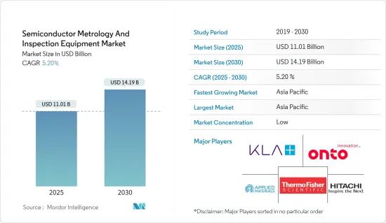
반도체 계측 및 검사 장비 시장 규모는 2025년 110억 1,000만 달러에 이르고, 2030년 141억 9,000만 달러에 달할 것으로 추정되며, 예측기간(2025-2030년)의 CAGR은 5.2%를 나타낼 것으로 전망됩니다.
주요 하이라이트
반도체 계측 및 검사는 반도체 제조 공정을 관리하는 데 중요한 역할을 합니다. 공정의 빠른 단계에서 단점이 발견되면, 그 후의 공정에 소비된 노력이 낭비될 수 있습니다.
하마마츠 포토닉스는 반도체 웨이퍼에 대한 현재 시장 요구를 충족시키기 위해 높은 생산 수율을 달성하는 것의 중요성을 강조하고 있습니다. 기타 가능한 결함을 효율적으로 특성 평가 및 측정하고, 모든 문제에 신속하게 대처하고, 고가의 다운타임을 최소한으로 억제하는 것이 매우 중요합니다.
반도체 계측은 웨이퍼의 물리적 특성에 대한 상세한 정보를 제공하고 특정 파라미터에 적합하도록 제조 공정의 조정을 용이하게 함으로써 반도체 제조 공정에 있어서 중요한 역할을 하고 있습니다.
반도체 부문은 성능과 속도를 향상시켜 보다 컴팩트한 집적회로를 목표로 하고 있으며, 그 결과 제조 기술도 진보하고 있습니다.
비용 효율적인 반도체 소재에 대한 수요는 스마트폰, 가전제품, 자동차용 용도에 의해 높아지고 있습니다. 바이스에 투자할 것으로 예상됩니다.스마트 디바이스의 이용은 증가 경향에 있어, 5G 접속의 세계의 확대와 함께 더욱 증가할 것으로 예상됩니다.
시장에서 확고한 발판을 구축하기 위해 벤더는 전략적 파트너십을 적극적으로 묶어 첨단 다기능 검사 플랫폼을 구축하고 있습니다. XRF(형광 X선)를 발표했습니다.이 툴은 광학적 방법으로는 확실히 측정할 수 없는 막두께를 정확하게 측정하기 위해 특별히 설계되어 있습니다.
그러나 예측 기간 동안 시장 성장은 셋업 비용의 높이나 계측 시스템의 취급에 관한 전문 지식의 부족 등의 요인에 의해 효율적으로 저해될 것으로 예상됩니다.
게다가 조사 대상 시장의 성장은 미국과 중국의 무역 분쟁 등의 거시 경제적 요인에 의해서도 과제가 되고 있습니다.
반도체 계측 및 검사 장비 시장 동향
큰 성장을 이루는 웨이퍼 검사
반도체 디바이스의 설계가 미세화됨에 따라 제조 수율 향상이라는 과제가 현저해지고 있습니다. 함량이나 전기적인 결함이 있으면 전체적인 생산 효율에 지장을 초래할 가능성이 있습니다.
웨이퍼 검사에 대한 수요 증가는 향후 수년간 3차원 집적 회로에 대한 요구 증가에 의해 촉진될 것으로 예상됩니다. 바이스에 널리 사용되고 있습니다.3차원 회로는 속도, 내구성, 저소비 전력, 메모리의 경량화 등, 제품 전체의 성능을 높이기 위해, 휴대가전, 센서, MEMS, 공업 제품 등, 스페이스에 제약이 있는 수많은 용도으로 인기를 모으고 있습니다.
비용 효율적인 클라우드 컴퓨팅 솔루션을 사용할 수 있게 되었기 때문에 마이크로프로세서 및 디지털 신호 프로세서와 같은 로직 디바이스에 대한 수요가 증가하고 있습니다. 확대되고 있는 것이 배경에 있습니다.또한, IoT 대응 디바이스의 보급에 의해 마이크로프로세서의 사용량도 증가하고 있습니다.
LED 용도에 300mm 웨이퍼가 널리 채용되고 있는 것도, 박형 웨이퍼 검사 시장의 세계의 성장을 가속하는 요인이 되고 있습니다.
SEMI Silicon Manufacturers 그룹(SMG)이 연말에 실시한 분석에 따르면 2023년 세계 실리콘 웨이퍼 출하량은 14.3% 감소했으며, 126억 200만 평방인치에 달했습니다.
5G의 도입 활동에 대한 투자 증가는 칩 산업에 있어서의 웨이퍼와 웨이퍼 검사 툴 수요를 한층 더 촉진할 것으로 예상됩니다. 2022에 따르면 북미는 향후 5년간 5G 가입 보급의 세계적 리더가 될 것으로 예측되고 있습니다.
IT, IoT, 재생 가능 에너지, EV, 전기 통신 및 기타 분야는 앞으로 몇 년 동안 크게 성장할 것으로 예상됩니다. 검사시장에는 많은 기회가 도입되고 있습니다.
아시아태평양이 시장을 독점
아시아태평양은 반도체 산업에서 제조와 소비의 양면에서 돌출한 지역 중 하나입니다. 비나 스마트폰 등의 전자기기에의 의존도의 높아짐과 함께, 이 지역에서의 웨이퍼 검사의 필요성을 높일 것으로 예상되고 있습니다. 또한, 이 지역에 위치하는 기업은 웨이퍼 검사의 이용을 향해 자금을 배분할 준비가 있습니다.
반도체 계측 및 검사 장비 시장에서는 많은 지역 기업들이 제휴와 파트너십을 맺고 있습니다. 예를 들어, 중국의 칩 생산 도구 제조업체인 선전 JT 자동화 장비는 중국 최대 칩 개발업체인 화웨이의 하이실리콘 테크놀로지스와 법적 구속력이 있는 5년(2021-2025년) 양해각서를 발표했습니다.
현지 반도체 산업을 발전시키기 위한 지역 정부의 이니셔티브도 연구 대상 시장의 성장에 유리한 전망을 창출하고 있습니다. 예를 들어, 중국 국무원의 '국가 집적 회로 산업 개발 가이드라인'은 2030년까지 이 국가를 반도체 산업의 전 분야에서 세계 리더로 만드는 것을 목표로 하고 있습니다. 게다가 '메이드 인 차이나 2025' 이니셔티브는 중국의 미래 경제에 필수적인 요소로 첨단 반도체 제조에 대한 지식의 달성을 유지하고 있습니다. 이것은 전국적인 강력한 제조업의 전략 구축에 매우 중점을 두고 있습니다.
예를 들어 2023년 7월 중국 2위 칩 파운드리인 화홍 반도체는 212억 위안(29억 5,000만 달러)을 조달할 계획을 밝혔습니다. 이 전략적 움직임은 반도체 공급의 자급 자족을 달성하고 미국의 기술 봉쇄를 극복하려는 중국의 단호한 노력을 따릅니다. 주로 칩 생산에 집중한 초기 단계와는 달리, 중국 IC 펀드 II는 기존의 장애를 극복하기 위해 국내 반도체 제조, 장비 및 관련 재료에 많은 투자를 했습니다.
미국과 중국의 긴장이 계속되고 있는 가운데, 한국은 자국의 반도체 산업을 강화하기 위해 자국판 「칩스법」의 제정을 계획하고 있습니다. 이러한 긴장은 조립과 패키징 등의 서비스에 대한 수요를 만들어내고 한국이 반도체 산업을 지원하는 것을 매우 중요하게 하고 있습니다. 2023년 3월 한국국회는 기업에 대한 세제우대조치와 투자의 장려를 통해 지배적인 반도체 산업을 강화하기 위한 법안을 통과했습니다. 이러한 정부의 대처에 의해 계측이나 검사 등의 백엔드 기기 제조업체가 이 지역에서 존재감을 높이는 기회가 늘어날 것으로 예상됩니다.
2023년 3월, 한국의 거대 전자 기업인 삼성은 2042년까지 용인 남사읍에 710만㎡ 규모의 대규모 반도체 허브를 구축하려는 한국 정부의 계획을 지원하기 위해 향후 20년간 300조 원(2,308억 달러 상당)을 투자하겠다고 발표했습니다. 이 전략적인 동향은 경쟁이 격화하는 세계 반도체 시장에 있어서의 한국의 지위를 강화하기 위한 것이며, 그 결과, 웨이퍼 테스트, ATP, 기타 장치 등의 백엔드 장치 수요를 밀어 올리게 됩니다.
게다가 많은 기업들이 다양한 분야에서 이익을 올리기 때문에 활동 확대에 주력하고 있습니다.
반도체 계측 및 검사 장비 산업의 개요
반도체 계측 및 검사 장비 시장은 다음과 같은 유명한 기업으로 구성되어 있습니다. 이러한 기업은 시장 확대와 인수에 주력함으로써 지속적으로 사업 규모를 확대해 왔습니다. 혁신을 추진하기 위해 연구개발 활동에 많은 자원을 투입하고 있습니다.
2023년 12월, 히타치 하이테크는 암시야 웨이퍼 결함 검사 장치의 최신 혁신인 DI4600을 발표했습니다. DI4600은 데이터 처리 능력이 강화되어 파티클과 결함의 검출 능력이 향상되고 있습니다.
어플라이드 머티리얼즈는 2023년 7월, 프라운호퍼 IPMS(포토닉 마이크로시스템 연구소)와 선구적인 협력 관계를 맺고 유럽에 반도체 계측 및 프로세스 해석의 최고봉 기술 센터를 설립한다고 발표했습니다. 이 혁신적인 허브는 최첨단 계측 시스템을 제공하여 반도체 연구를 가속화하고 유럽 전역의 칩 제조업체 및 에코시스템 파트너와의 개발 노력을 강화하기 위해 설계되었으며, 특히 ICAPS(사물 인터넷, 통신, 자동차, 전력 및 센서) 시장 부문에 중점을 두고 있습니다.
The Semiconductor Metrology And Inspection Equipment Market size is estimated at USD 11.01 billion in 2025, and is expected to reach USD 14.19 billion by 2030, at a CAGR of 5.2% during the forecast period (2025-2030).
Key Highlights
Semiconductor metrology and inspection play a crucial role in the management of the semiconductor manufacturing process. The manufacturing process of semiconductor wafers involves approximately 400 to 600 steps, which can be completed within one to two months. Any shortcomings detected early on in the process can result in the wastage of all the efforts put into the subsequent steps. Metrology and inspection procedures are implemented at critical junctures of the semiconductor manufacturing process to guarantee a specific yield.
Hamamatsu emphasizes the importance of achieving high production yields in order to satisfy the current market requirements for semiconductor wafers. Metrology and inspection play a vital role in the extensive semiconductor manufacturing process to guarantee optimal quality and yield. It is crucial to efficiently characterize and measure thin films, line widths, pattern flaws, and other possible defects to promptly address any issues and minimize expensive downtime. In semiconductor inspection, the utilization of higher radiance UV light sources is essential to reduce inspection durations and improve the precision of evaluating patterns and thin films on wafers.
Semiconductor metrology plays a crucial role in the semiconductor manufacturing process by offering detailed information on the physical properties of the wafer and facilitating adjustments to the production process to meet specific parameters. This ensures the production of reliable semiconductor devices of high quality while minimizing wastage, thus maintaining the economic viability and sustainability of the manufacturing process.
The semiconductor sector is continuously aiming for more compact integrated circuits that provide enhanced performance and speeds, resulting in progress in manufacturing techniques. Maintaining accurate oversight of procedures has emerged as a vital factor in manufacturing. With firms like TSMC, Infineon, Qualcomm, and Intel expanding their chip production investments, the demand for metrology equipment and services is expected to rise in the back-end process.
The demand for cost-effective semiconductor materials is being fueled by smartphones, consumer electronics, and automotive applications. These advancements are inspiring innovations like wireless technologies (5G) and artificial intelligence. Additionally, the semiconductor industry is expected to invest in IoT devices to achieve smart products as the trend of adoption of IoT devices continues to grow. The utilization of smart devices is on the rise and is anticipated to increase further with the global expansion of 5G connections. As per the GSMA, it is estimated that 5G mobile broadband connections will reach 1,100 million (1.1 billion) by the year 2025, while the 5G deployment is expected to encompass 34% of the global population by the same year.
In order to gain a strong foothold in the market, vendors are actively engaging in strategic partnerships to create advanced multifunction inspection platforms. Recently, k-Space Associates introduced its latest thin film metrology tool, the kSA XRF (X-ray fluorescence), in January 2023. This tool is specifically designed to accurately measure the thickness of films that cannot be reliably measured using optical methods. Its effectiveness has been demonstrated in measuring semiconductor and dielectric layers on various substrates such as glass panels, wafers, and susceptors. These applications are particularly relevant in the fields of solar energy, power generation, and other thin-film technologies.
However, the market's growth during the forecast period is expected to be hindered efficiently by factors such as high setup costs and a lack of expertise in handling metrology systems. In order to overcome these challenges, service-oriented players are offering on-demand metrology services, providing a professional extension in the specialized field of precision dimensional metrology.
Furthermore, the growth of the market studied is also challenged by macroeconomic factors, such as the US-China trade dispute. The United States has imposed several sanctions on China, preventing the country from accessing advanced semiconductor equipment. Since China plays a significant role in the market's supply chain, these trends negatively impact the growth of the market studied.
Semiconductor Metrology and Inspection Equipment Market Market Trends
Wafer Inspection to Witness Significant Growth
As the design of semiconductor devices progresses toward smaller nodes, the challenge of increasing manufacturing yields becomes more pronounced. The introduction of smaller nodes and intricate 3D architectures leads to additional steps and heightened complexity in the design phase. With hundreds of steps in the process, any defect or electrical fault at any stage can impede overall production efficiency. Given the significance of time-to-market and time-to-yield in determining the success of a new semiconductor design, the utilization of wafer inspection tools is crucial to ensure optimal performance at each stage.
The growing demand for wafer inspection is expected to be fueled by the increasing need for three-dimensional integrated circuits in the upcoming years. These circuits are widely used in small semiconductor devices such as memory cards, smartphones, smart cards, and various computing devices. Three-dimensional circuits are gaining popularity in numerous space-constrained applications like portable consumer electronics, sensors, MEMS, and industrial products, as they enhance overall product performance in terms of speed, durability, low power consumption, and lightweight memory.
The increasing availability of cost-effective cloud computing solutions has led to a rise in demand for logic devices such as microprocessors and digital signal processors. This is primarily driven by the growing use of server and data center systems in various industries. Furthermore, the proliferation of IoT-enabled devices has resulted in a higher usage of microprocessors. Thin wafers are increasingly utilized in these devices to enhance temperature control and optimize performance. These factors collectively contribute to the expansion of the wafer inspection market.
The widespread adoption of 300 mm wafers in LED applications is also a key driver for the global growth of the thin wafer inspection market. These wafers offer higher yields, enabling LED manufacturers to achieve economies of scale and enhance profitability. As the number of operational 300 mm wafer production facilities continues to increase, the demand for 300 mm wafers is expected to witness a significant surge.
According to the year-end analysis conducted by the SEMI Silicon Manufacturers Group (SMG), global silicon wafer shipments experienced a decline of 14.3% in 2023, reaching 12,602 million square inches. Additionally, wafer revenue contracted by 10.9% to USD 12.3 billion during the same period. However, there is optimism for the future as the momentum from the 2024 rebound is expected to continue until 2026. This positive trend is anticipated to result in new record-high wafer shipments, driven by the increasing demand for silicon in various sectors such as artificial intelligence (AI), high-performance computing (HPC), 5G, automotive, and industrial applications.
The introduction of 5G and increasing investments in the 5G adoption activities are further expected to drive the demand for wafers and wafer inspection tools in the chip industry. According to the Ericsson Mobility Report 2022, North America is projected to be the global leader in 5G subscription penetration over the next five years. It is anticipated that 90% of subscriptions in the region will be 5G by 2027. Additionally, the report predicts that by 2027, 82% of subscriptions in Western Europe, 80% in the Gulf Cooperation Council, and 74% in North-East Asia will be 5G. In India, where 5G deployments have already begun, it is expected that 5G will account for approximately 40% of all subscriptions by 2027. Globally, 5G is expected to represent nearly half of all subscriptions by 2027, reaching a total of 4.4 billion subscriptions.
The IT, IoT, renewable, EVs, telecom, and other sectors are poised for substantial growth in the upcoming years. Additionally, these sectors heavily rely on wireless technology. The utilization of ICs and semiconductors enables the application of wireless technology. As a result, the wafer inspection market is presented with a multitude of opportunities. Prominent companies in the semiconductor industry, such as Infineon, TSMC, ST, Micron, Intel, Samsung, and others, are making significant investments in chip production activities, which can greatly contribute to the market's increased demand.
Asia-Pacific to Dominate the Market
Asia-Pacific is one of the prominent regions in the semiconductor industry in terms of manufacturing and consumption. According to SIA, Asia-Pacific is the largest regional semiconductor market, and China accounts for the most significant share in the region. The significant advancements in the electronics sector, combined with the growing reliance on electronic gadgets like televisions and smartphones, are anticipated to boost the requirement for wafer inspection in the region. Furthermore, companies situated in this area are prepared to allocate funds toward the utilization of wafer inspections.
Many regional companies are entering collaborations and partnerships in the semiconductor metrology/inspection equipment market. For instance, Shenzhen JT Automation Equipment, a chip production tool manufacturer in China, announced a legally binding five-year (2021-2025) memorandum of understanding with Huawei's HiSilicon Technologies, China's largest chip developer. Both firms aim to extend their partnership for the development of semiconductor packaging tools, creating a self-sufficient and regulated industry.
The regional government's initiatives to develop the local semiconductor industry also create a favorable outlook for the growth of the market studied. For instance, China's State Council's "National Integrated Circuit Industry Development Guidelines" aim to make the country a global leader in all segments of the semiconductor industry by 2030. Additionally, the Made in China 2025 initiative maintains achieving knowledge concerning advanced semiconductor manufacturing as a vital component of China's future economy. It is highly focused on building a strategy for strong manufacturing nationwide.
For instance, in July 2023, Hua Hong Semiconductor, the second-largest chip foundry in China, revealed its plan to raise CNY 21.2 billion (USD 2.95 billion). This strategic move is in line with China's determined efforts to attain self-sufficiency in semiconductor supply and overcome the technology blockade imposed by the United States. In contrast to the initial phase that primarily concentrated on chip production, the China IC Fund II has made significant investments in domestic semiconductor manufacturing, equipment, and associated materials to overcome the existing obstacles.
South Korea plans to enact its own version of the "Chips Act" in order to bolster its semiconductor industry amid the ongoing tensions between the United States and China. These tensions have created a demand for services such as assembly and packaging, making it crucial for South Korea to support its semiconductor industry. In March 2023, the country's parliament passed legislation to strengthen its dominant semiconductor industry by providing tax benefits to businesses and encouraging investments. Such government initiatives are expected to boost the opportunities for the backend equipment markers, such as metrology and inspection, to enhance their presence in the region.
In March 2023, Samsung, the Korean electronics giant, announced its intention to invest KRW 300 trillion (equivalent to USD 230.8 billion) over the next two decades in support of the South Korean government's initiative to establish a massive semiconductor hub spanning 7.1 million square meters in Namsayup, Yongin, by 2042. This strategic move is designed to bolster Korea's position in the increasingly competitive global semiconductor market, consequently driving up the demand for backend equipment such as wafer testing, ATP, and other equipment.
Additionally, numerous enterprises are focusing on expanding their activities to boost profits in different sectors. The New Taipei City government announced that ASML Holding NV, a Dutch company that specializes in semiconductor equipment, will commence the construction of its new facility in the Linkou District of New Taipei City in the fiscal year 2024. Moreover, Tokyo Electron Ltd, a Japanese electronics and semiconductor corporation, is making progress in establishing its operations hub in the Southern Taiwan Science Park in Tainan, with plans to complete it by the end of 2024. These investments have the potential to create opportunities in the metrology and inspection market.
Semiconductor Metrology and Inspection Equipment Industry Overview
The semiconductor metrology and inspection equipment market comprises prominent players such as Applied Materials Inc., Nikon Metrology NV, and KLA Corporation. These firms have continuously expanded their operation scales by focusing on market expansions and acquisitions. Acquisition activities effectively set the ball rolling regarding the overall growth of the market studied. Large companies have also been expending significant resources on R&D operations to protect their market position and drive innovation in the market studied. Overall, the degree of competition remains high, primarily driven by the strong presence of prominent players involved in the market studied.
In December 2023, Hitachi High-Tech Corporation unveiled the DI4600, the latest innovation in its Dark Field Wafer Defect Inspection System. This state-of-the-art tool is specifically designed to inspect particles and defects on patterned wafers in semiconductor production lines. With its dedicated server, the DI4600 offers enhanced data processing power, enabling improved detection capabilities for particles and defects. By incorporating this advanced system into their production lines, semiconductor manufacturers can ensure highly accurate defect monitoring, resulting in increased yields and cost efficiency as production volumes continue to rise.
In July 2023, Applied Materials Inc. and the Fraunhofer Institute for Photonic Microsystems IPMS announced a pioneering collaboration to create the premier technology center for semiconductor metrology and process analysis in Europe. This innovative hub is designed to provide state-of-the-art metrology systems to accelerate semiconductor research and enhance development efforts with chipmakers and ecosystem partners across Europe, with a specific focus on ICAPS (Internet of Things, communications, automotive, power, and sensors) market segments.
Additional Benefits:
The market estimate (ME) sheet in Excel format
3 months of analyst support
TABLE OF CONTENTS
1 INTRODUCTION
1.1 Study Assumptions and Market Definition
1.2 Scope of the Study
2 RESEARCH METHODOLOGY
3 EXECUTIVE SUMMARY
4 MARKET INSIGHTS
4.1 Market Overview
4.2 Industry Attractiveness - Porter's Five Forces Analysis
4.2.1 Bargaining Power of Suppliers
4.2.2 Bargaining Power of Buyers
4.2.3 Threat of New Entrants
4.2.4 Threat of Substitutes
4.2.5 Degree of Competition
4.3 An Assessment of the Impact of Key Macro Trends
5 MARKET DYNAMICS
5.1 Market Drivers
5.1.1 Increasing Demand for High-performance, Low-cost Semiconductors
5.1.2 Increasing Demand for Semiconductor Wafers in Consumer Electronics
5.2 Market Restraints
5.2.1 High Setup Cost and Lack of Expertise in Handling Metrology Systems Efficiently