


반도체 에칭 장비 시장은 2025년 254억 달러에서 2026년에는 273억 3,000만 달러로 성장하며, 2026-2031년에 CAGR 7.60%로 추이하며, 2031년까지 394억 3,000만 달러에 달할 것으로 예측됩니다.

이러한 성장은 첨단 공정 노드에서의 지속적인 설비 투자, 게이트 올 어라운드 트랜지스터의 채택 가속화, 그리고 광범위한 이기종 통합의 확산을 반영합니다. 인공지능 워크로드 증가, 전기자동차 생산 확대, 국가 보조금 프로그램이 설치된 장비의 잠재적 시장 규모를 지속적으로 확대하는 한편, 지속적인 헬륨 부족과 수출 관리 규제가 투자 시점에 영향을 미치고 있습니다. 로직 및 마이크로프로세서 제조 공장은 출하량 기준으로 가장 큰 점유율을 차지하는 가장 장비 집약적인 고객이지만, 데이터센터 사업자들의 높은 대역폭과 향상된 에너지 효율성에 대한 요구로 인해 고 대역폭 메모리 및 첨단 패키징 라인이 가장 빠른 성장세를 보이고 있습니다. 기록하고 있습니다. 원자층 에칭 플랫폼이 가장 높은 매출 성장률을 보이고 있지만, 유도 결합 플라즈마 장비는 처리량과 화학적 유연성으로 인해 여전히 대량 생산 라인의 기반이 되고 있습니다. 지역별로는 아시아태평양이 설치 용량을 주도하고 있지만, 북미, 유럽, 중동의 보조금 지원 팹 프로젝트가 진행되면서 반도체 에칭 장비 시장의 지역적 분포가 꾸준히 다양화되고 있습니다.
로직 회로의 미세화가 진행됨에 따라 팹에서는 플라즈마에 의한 손상을 억제하면서 원자 수준의 치수 제어를 실현하는 에칭 장비의 도입이 요구되고 있습니다. 삼성의 3nm 게이트 올어라운드 디바이스 양산과 TSMC의 N2 공정 인증으로 단분자층 단위로 재료를 제거하는 원자층 에칭 챔버에 대한 즉각적인 수요가 증가하고 있습니다. 어플라이드 머티어리얼즈와 램리서치는 독자적인 펄스 플라즈마 사이클과 인서튜메트리 기술을 통해 서브나노미터 수준의 변동률 예산을 달성하고 있으며, 소규모 업체들이 동등한 수준의 R&D 자금을 조달하기 어려운 상황에서 경쟁 우위를 강화하고 있습니다. 인텔의 18A 로드맵은 더욱 엄격한 프로파일 제어를 요구하고 있으며, 이러한 노드에 대응하는 공급업체들에게 다년간 수요 전망을 확고히 하고 있습니다. 노드 전환에 따라 고유전율 절연체, 루테늄 배리어층 등으로의 필름 적층화가 진행되는 가운데, 차별화된 화학처리 기술은 팹 측의 전환 비용을 더욱 높여 주요 장비 업체들의 가격 결정력을 강화하고 있습니다.
중국의 로직 및 특수 파운드리 업체들은 업계 전반의 경기 둔화에도 불구하고 2024년에월약 20만 개의 웨이퍼를 추가할 것으로 예상되며, 이는 전 세계 증설량의 약 15%에 해당합니다. 정부의 자본 투입과 유리한 토지 임대 조건이 신규 공장 건설을 가속화하는 한편, 수출 라이선스의 불확실성으로 인해 사업자들은 장비 납기를 앞당기고 있습니다. NAURA 등 국내 유수의 업체들이 중급 노드용 에칭 장비 공급 점유율을 확대하고 있지만, 최첨단 노드용 주문의 대부분은 여전히 해외 유수의 업체들이 차지하고 있습니다. 규제 변경에 대비한 비축으로 업계 전반의 침체기에도 분기별 수주량은 높은 수준을 유지하여 반도체 에칭 장비 시장은 일반적인 경기 침체의 영향을 완화하고 있습니다.
메모리 제조업체들은 과잉 생산능력을 해소하기 위해 주기적으로 설비투자 예산을 삭감합니다. SK하이닉스, 마이크론, 삼성은 공급과잉에 따라 2024년 초 에칭 장비 구매를 약 25% 줄이고, 분기별 장비 출하량을 억제했습니다. 3D NAND 적층에는 200회 이상의 에칭 공정이 필요하므로 지출 중단은 에칭 장비 공급업체의 매출에 특히 큰 영향을 미칩니다. 로직 분야가 일부 상쇄하는 것, 메모리 재활용의 변동폭은 벤더의 생산 계획에 변동을 가져옵니다.
2025년 반도체 에칭 장비 시장 규모의 36.65%를 로직 마이크로프로세서 제조 공장이 차지하며, 3nm 이하 미세구조로의 전환 속도가 가장 빠르다는 점에서 선두를 유지했습니다. 새로운 공정 노드마다 프로파일 제어 정밀도가 요구되므로 웨이퍼 당 에칭 비용이 증가합니다. 스마트폰과 데이터센터의 지속적인 업데이트 주기가 웨이퍼 생산량을 늘리는 한편, 자동차 자율주행용 혼합 신호 칩이 생산량에 추가적으로 기여하고 있습니다. 메모리 용량 증설은 여전히 간헐적이지만, 230단 이상의 3D NAND는 딥 그루브 에칭 수요를 지속하고 있습니다. 첨단 패키징 및 고대역폭 메모리 라인은 2031년까지 연평균 복합 성장률(CAGR) 8.79% 성장할 것으로 예상되며, 로직 다이와 적층형 DRAM을 결합한 AI 가속기 수요 증가에 따른 수혜를 받을 것으로 예측됩니다.
팹리스 반도체 제조업체들이 위험분담 모델을 추구하는 가운데 파운드리 서비스가 주목받고 있으며, TSMC는 2025년 말까지 CoWoS 패키징의월생산능력을 65,000 웨이퍼로 확대할 것으로 예상하고 있습니다. 전력 디바이스 및 개별 디바이스는 전기자동차용 인버터 및 급속 충전기에 SiC 스위치의 채택이 확대됨에 따라 가속화되고 있으며, 전용 심도 반응성 이온 에칭 시스템을 필요로 합니다. MEMS 및 센서 제조업체들은 저압 플라즈마 모듈을 마이크 어레이 및 타이어 공기압 모니터에 활용하고 있습니다. 신흥 광-양자 소자는 현재로서는 틈새 시장이지만, 원자 수준의 에칭 선택성이 요구되어 공급업체가 차별화할 수 있는 새로운 길을 열어주고 있습니다.
유도결합 플라즈마 장비는 2025년 매출의 33.25%를 차지하며, 양산 팹의 핵심 장비로서 입지를 확고히 하고 있습니다. 광범위한 화학적 처리 능력으로 단일 플랫폼에서 폴리실리콘, 고유전율 절연체, 금속 게이트에 대응할 수 있으며, 라인 유지보수를 간소화할 수 있습니다. 반응성 이온 에칭 장비는 종횡비 제약이 완만한 후공정 노드에서 계속 채택되고 있습니다. 딥 RIE 장비는 MEMS, 관통형 실리콘 비아(TSV) 등 특수한 분야를 공략하고 있으며, 틈새 시장 공략을 통해 높은 이익률을 유지하고 있습니다.
반도체 에칭 장비 시장이 옹스트롬 수준의 제어로 전환하는 가운데, 원자층 에칭 플랫폼은 9.01%의 연평균 복합 성장률(CAGR)로 가장 높은 성장률을 기록했습니다. 어플라이드 머티어리얼즈(Applied Materials)는 사이클 당 단일 분자층을 제거하는 펄스 고주파 단계를 홍보하고 있습니다. 고종횡비 모듈은 60:1 이상의 3D NAND 트렌치를 지원하며, 여기서 발생하는 측벽 뒤틀림이 셀 효율을 저해할 수 있습니다. 등방성 세정 및 본딩 전 표면 처리에는 여전히 습식 벤치 시스템이 사용되지만, 플라즈마 화학 처리가 더 부드럽고 선택성이 높아짐에 따라 총 점유율이 감소하고 있습니다.
아시아태평양은 2025년 매출의 70.85%를 차지할 것으로 예상되며, 대만, 한국, 중국 본토에서 수십억 달러 규모의 생산능력 증설이 지속될 것으로 예측됩니다. TSMC의 CoWoS(Chip-on-Wafer-on-Socket) 생산 능력이월6만 5,000장까지 확대된 것은 첨단 패키징 분야에서 지역 주도권을 확보한 것을 의미합니다. 한편, 삼성과 SK하이닉스의 DRAM 및 NAND 사이클은 대규모 에칭 수요를 지속적으로 견인하고 있습니다. 중국 국내 업체들은 빠르게 학습 곡선을 오르고 있으며, NAURA의 44% 이익 성장과 세계 6위권 진입은 이러한 진전을 지원하고 있습니다.
북미의 점유율은 500억 달러가 넘는 CHIPS 법의 특혜에 의해 지원되고 있습니다. 인텔의 오하이오주 200억 달러 규모의 건설 프로젝트와 TSMC의 애리조나 공장이 대형 멀티 챔버 에칭 장비 수주를 주도하고 있으며, 공급업체들의 수주 잔고가 아시아 의존도에서 분산되고 있습니다. 유럽의 칩스법 자금은 독일, 프랑스, 아일랜드의 프로젝트를 추진하고 있으며, 2020년 말까지 장비 출하 전망을 확대하고 있습니다.
중동 및 아프리카은 정부의 전략적 자율성 추구로 인해 10.74%의 가장 높은 예측 CAGR을 나타낼 것으로 보입니다. 사우디아라비아의 NEOM 캠퍼스와 아랍에미리트의 클린룸 계획에는 턴키 에칭 모듈을 도입하는 파일럿 라인이 계획되어 있습니다. 인프라 부족과 인력 부족은 여전히 문제이지만, 지속적인 공공 자금 지원은 세계 공급업체를 유치하여 반도체 에칭 장비 시장의 지역적 기반을 더욱 확장하고 있습니다.
The semiconductor etch equipment market is expected to grow from USD 25.4 billion in 2025 to USD 27.33 billion in 2026 and is forecast to reach USD 39.43 billion by 2031 at 7.60% CAGR over 2026-2031.
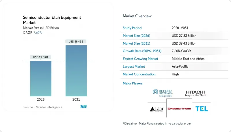
This growth reflects sustained capital spending at advanced process nodes, accelerating adoption of gate-all-around transistors, and wider deployment of heterogeneous integration. Rising artificial-intelligence workloads, expanding electric-vehicle production, and national subsidy programs continue to enlarge the addressable base of installed tools, while persistent helium shortages and export-control rules shape investment timing. Logic and microprocessor fabs remain the most equipment-intensive customers, commanding the largest share of shipments, yet high-bandwidth-memory and advanced-packaging lines post the fastest unit growth as data-center operators require higher bandwidth and improved energy efficiency. Atomic-layer-etch platforms record the highest revenue momentum, but inductively coupled plasma tools still anchor high-volume manufacturing lines because of their throughput and chemistry flexibility. Regionally, Asia-Pacific dominates installed capacity, although subsidy-backed fab projects in North America, Europe, and the Middle East steadily diversify the geographic footprint of the semiconductor etch equipment market.
Shrinking logic geometries compel fabs to adopt etchers that deliver atomic-level dimensional control while limiting plasma-induced damage. Samsung's volume ramp of 3 nm gate-all-around devices and TSMC's N2 process qualification amplify immediate demand for atomic-layer-etch chambers that remove material one monolayer at a time. Applied Materials and Lam Research deploy proprietary pulsed-plasma cycles and in-situ metrology to meet sub-nanometer variability budgets, which strengthens their competitive moat as smaller vendors struggle to fund similar R&D. Intel's 18A roadmap extends the requirement for even tighter profile control, anchoring multi-year visibility for suppliers positioned on these nodes. As node migration pushes film stacks toward high-k dielectrics and ruthenium barriers, differentiated chemistries further raise switching costs for fabs and reinforce pricing power for leading toolmakers.
Chinese logic and specialty foundries added roughly 200,000 wafer starts per month in 2024, equal to nearly 15% of global build-out, despite broader cyclical softness. Government equity injections and advantageous land leasing accelerate greenfield construction, while export-license uncertainty prompts operators to front-load equipment receipts. Domestic champions such as NAURA supply an expanding share of mid-node etchers, but tier-one foreign vendors still capture most advanced-node orders. Stockpiling ahead of anticipated rule changes keeps quarterly bookings elevated even during industry pauses, cushioning the semiconductor etch equipment market against typical downturns.
Memory producers periodically slash equipment budgets to correct overcapacity. SK Hynix, Micron, and Samsung cut etch purchases by nearly 25% in early 2024 following a supply glut, dampening quarterly tool shipments. Because 3D NAND stacks require more than 200 etch passes, each spending pause disproportionately weights the revenue of etch suppliers. Although the logic segment provides a partial offset, the amplitude of memory cycles injects volatility into production planning for equipment vendors.
Other drivers and restraints analyzed in the detailed report include:
For complete list of drivers and restraints, kindly check the Table Of Contents.
Logic and microprocessor fabs accounted for a 36.65% share of the semiconductor etch equipment market size in 2025, securing that primacy by migrating fastest toward sub-3 nm structures. Each new node requires tighter profile control, thereby boosting per-wafer etch spend. Continuous smartphone and data-center refresh cycles reinforce wafer starts, while mixed-signal chips for automotive autonomy add incremental volume. Memory capacity additions remain episodic, but 3D NAND layer counts above 230 sustain deep-trench etch demand. Advanced packaging and high-bandwidth-memory lines, projected to grow at an 8.79% CAGR through 2031, gain from AI accelerators that pair logic dies with stacked DRAM.
Foundry services attract fabless chipmakers seeking risk-sharing models, pushing TSMC to expand CoWoS packaging output to 65,000 wafers per month by late 2025. Power and discrete devices accelerate as electric-vehicle inverters and fast chargers embed more SiC switches, drawing specialized deep-reactive-ion systems. MEMS and sensor makers exploit low-pressure plasma modules for microphone arrays and tire-pressure monitors. Emerging photonic and quantum devices, though presently niche, demand atomic-level etch selectivity, offering new avenues for supplier differentiation.
Inductively coupled plasma tools delivered 33.25% of 2025 revenue, cementing their status as the backbone of high-volume fabs. Their broad chemistry range allows one platform to tackle polysilicon, high-k dielectrics, and metal gates, simplifying line maintenance. Reactive-ion systems retain service in trailing nodes where aspect-ratio constraints are modest. Deep-RIE tools capture specialty segments such as MEMS and through-silicon-vias, commanding premium margins for their niche capability.
Atomic-layer-etch platforms record the highest growth at a 9.01% CAGR as the semiconductor etch equipment market pivots toward angstrom-level control. Applied Materials advertises pulsed radio-frequency steps that remove a single monolayer per cycle. High-aspect-ratio modules tackle 3D NAND trenches exceeding 60:1, where sidewall bowing can cripple cell efficiency. Wet-bench systems persist for isotropic cleans and pre-bond surface prep, yet their total share erodes as plasma chemistries grow gentler and more selective.
The Semiconductor Etch Equipment Market Report is Segmented by Application (Logic/MPU, Memory, and More), Equipment Type (Reactive Ion Etcher, ICP Etcher, Deep RIE, Wet Etch Systems, High-Aspect-Ratio Etch, and Atomic Layer Etch), Etching Technology (Dry Etch and Wet Etch), Process Type (Front-End-Of-Line (FEOL) Etching and Back-End-Of-Line (BEOL) Etching), and Geography. The Market Forecasts are Provided in Terms of Value (USD).
Asia-Pacific generated 70.85% of 2025 revenue as Taiwan, South Korea, and mainland China sustained multi-billion-dollar capacity additions. TSMC's CoWoS expansion to 65,000 wafers per month illustrates regional leadership in advanced packaging, while Samsung and SK Hynix cycles in DRAM and NAND continue to command large etch volumes. Domestic Chinese vendors climb the learning curve rapidly; NAURA's 44% profit growth and move into the global top-six underlines this progress.
North America's share is buoyed by CHIPS Act incentives exceeding USD 50 billion. Intel's USD 20 billion Ohio build and TSMC's Arizona site pull large multi-chamber etch orders, diversifying supplier backlog away from sole reliance on Asia. European Chips Act funds steer projects in Germany, France, and Ireland, extending visibility for equipment shipments through decade-end.
The Middle East and Africa record the fastest projected CAGR at 10.74% as governments seek strategic autonomy. Saudi Arabia's NEOM campus and the United Arab Emirates' clean-room programs commit to pilot lines that import turnkey etch modules. Infrastructure gaps and talent shortages remain hurdles, yet sustained public funding attracts global suppliers, further widening the geographic base of the semiconductor etch equipment market.