


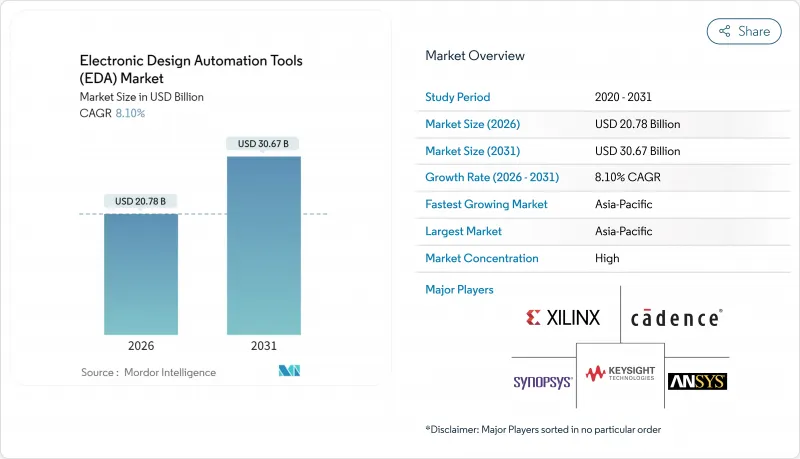
전자 설계 자동화 도구(EDA) 시장 규모는 2026년 207억 8,000만 달러로 평가되었고, 2025년 192억 2,000만 달러에서 성장할 전망입니다.
2031년 예측은 306억 7,000만 달러에 이를 것으로 예상되며, 2026-2031년에 걸쳐 연평균 복합 성장률(CAGR) 8.1%로 성장할 전망입니다.

이 전망은 더 빠른 트랜지스터 미세화, AI 기반 설계 흐름, 파운드리-도구 간 긴밀한 협력을 기반으로 합니다. 칩 설계자들은 수동 규칙 조정에서 데이터 기반 최적화로 전환하며 테이프아웃 주기를 단축하고 재설계 위험을 낮추고 있습니다. 클라우드 기반 용량 급증은 고급 검증 접근성을 확대하는 한편, 자동차 기능 안전 규제는 형식적 방법을 주류 설계로 진입시키고 있습니다. 2025년 완료 예정인 시놉시스(Synopsys)의 앤시스(Ansys) 350억 달러 인수 거래는 실리콘, 패키지, 전체 시스템 성능을 동시에 공동 최적화할 수 있는 통합형 디바이스-투-시스템 플랫폼으로의 체계적 전환을 시사합니다. 한편, 지정학적 수출 통제는 병행 EDA 생태계를 촉진하여 공급업체들이 수익 감소를 피하기 위해 여러 지역 파운드리용 설계 흐름을 인증하도록 강제하고 있습니다.
게이트-올-어라운드 트랜지스터, 백사이드 전원 공급, 멀티다이 패키징은 7nm 공정 대비 설계 규칙 검사(DRC)를 10배 증가시킵니다. 파운드리 업체들은 이제 EDA 선도 기업들과 공통 워크플로우를 공동 개발 중이며, 시노프시스와 TSMC는 2025년 4월 A16 및 N2P 노드용 완전한 디지털 및 아날로그 툴체인을 인증했습니다. 통합된 탐색-사인오프 환경은 비용이 많이 드는 재설계(3nm 공정 기준 5천만 달러 이상)를 줄여줍니다. 인텔의 18A 프로그램 역시 단일 기판에 컴퓨팅, 메모리, I/O를 통합하는 2.5D/3D 아키텍처를 위한 통합 흐름에 의존합니다.
하이퍼스케일 및 엣지 공급업체들은 목적에 특화된 추론용 실리콘을 점점 더 많이 의뢰하고 있습니다. 캐던스는 2025년 1분기 반도체 IP 매출이 전년 동기 대비 40% 성장했으며, 이 같은 성장세는 AI 및 칩렛 프로젝트 덕분이라고 밝혔습니다. 엔비디아, ASML, TSMC, 시노프시스는 CuLitho 소프트웨어 스택을 통해 리소그래피 시뮬레이션 속도가 40배 향상되었다고 보고했으며, 이는 AI 전력 효율성 목표를 충족하는 레티클 레이아웃을 가능하게 합니다. 가속기 이질성이 증가함에 따라 SIP 재사용 및 패키지 내 상호 연결 표준은 IP 검증 수요를 더욱 촉진하고 있습니다.
포괄적인 3nm 사인오프를 위한 연간 기업용 번들 비용이 이제 좌석당 100만 달러를 초과하여, 중견 팹들은 도구 모듈을 우선순위로 정하고 리프레시 주기를 연장해야 하는 상황에 직면했습니다. 과점적 공급 구조로 인해 공급업체의 가격 결정력이 유지되며, 특히 오픈소스 대체재가 없는 타이밍 클로저 및 리소그래피 시뮬레이션 패키지의 경우 더욱 그러합니다.
반도체 지적 재산권(SIP)은 검증된 인터페이스 블록과 혼합 신호 코어를 선호하는 칩릿 아키텍처의 증가로 인해 도구 카테고리 중 가장 빠른 9.7%의 연평균 성장률(CAGR)을 기록할 것으로 전망됩니다. 2025년 SIP는 전자 설계 자동화 도구 시장 매출의 18.74%를 차지했으나, 파운드리 업체들이 ‘알려진 양품 다이(known-good-die)’ 전략을 추진함에 따라 프로젝트당 적용률은 2023년 대비 두 배로 증가했습니다. SIP 애플리케이션의 전자 설계 자동화 도구 시장 규모는 2031년까지 상당한 성장률을 보일 것으로 예상되며, 이는 단일 칩 SoC에서 이종 어셈블리로의 전환을 강조합니다.
IC 물리 설계 및 검증은 배치, 라우팅, 정적 타이밍, DRC가 모든 테이프아웃에서 필수적이라는 특성 덕분에 35.82%의 점유율을 유지했습니다. 그러나 AI 강화 플로어플래닝은 다중 목표 최적화를 자동화하여 최근 3nm 설계에서 처리 시간을 30% 단축시켰습니다.
프론트엔드 설계 도구는 고수준 합성(HLS) 및 자연어-RTL 변환 생성기의 생산성 향상으로 9.35%의 연평균 성장률(CAGR)을 기록했습니다. RTL 자동화 분야의 전자 설계 자동화 도구 시장 규모는 기능적 의도를 더 적은 반복으로 포착하는 AI 지원 코드 생성에 힘입어 2031년까지 크게 성장할 것으로 전망됩니다. 레이아웃, 라우팅 및 타이밍 클로저는 여전히 전자 설계 자동화 도구 시장 점유율의 32.10%를 차지하며, 이는 최종 검증 수준의 타이밍 수렴 및 고급 3D 기생 추출의 대체 불가능한 특성을 반영합니다.
생성형 설계 플랫폼은 이제 인간 스크립트 대비 배선 길이를 11%, 누설 전류를 9% 감소시키는 배치 지침을 생성합니다. 그러나 최종 SOC 인도는 여전히 파운드리에서 승인하는 검증된 타이밍 및 전기 규칙 보고서에 의존하여 기존 백엔드 툴체인의 중요성을 공고히 합니다.
전자 설계 자동화 도구(EDA) 보고서는 도구 유형(컴퓨터 지원 설계, IC 물리 설계 및 검증 등), 설계 흐름 단계(프론트엔드 설계 RTL 등), 도입 형태(온프레미스, 클라우드 기반 등), 최종 사용자 업계(통신 인프라, 소비자 가전 등), 지역(북미 등)별로 분류되어 있습니다. 시장 예측은 금액(달러)으로 제공됩니다.
아시아태평양 지역은 2025년 42.05%의 점유율을 기록했으며, 2031년까지 연평균 9.55% 성장률을 보일 전망입니다. 대만과 한국의 파운드리 집적화가 지역 내 툴 수요를 견인하는 가운데, 중국은 미국의 수출 통제에 대응해 자국 EDA 스택 구축을 가속화하고 있습니다. 국가 주도의 이니셔티브는 3nm 생산 확대 전 공정 흐름 현지화를 목표로 AI 지원 배치-배선 엔진 및 SPICE 시뮬레이터에 보조금을 집중하고 있습니다. 인도는 대규모 엔지니어링 기반을 활용하며, 서구 고객사의 비용 효율적인 RTL 및 DFT 지원 수요 증가로 2024년 현지 설계 서비스 기업이 17% 성장했습니다.
북미는 AI 알고리즘, IP 카탈로그, 클라우드 인프라 분야의 리더십을 통해 영향력을 유지하고 있습니다. 2025년 북미 지역 점유율은 29.15%로 소폭 감소했으나, 최첨단 노드용 레퍼런스 툴 흐름의 주요 공급처 지위는 유지됩니다. 수출 통제 제도로 인해 공급업체들은 라이선스 키 지오펜싱을 구현해야 하며, 이는 규정 준수 비용을 증가시키지만 동시에 북미 IP 체인을 고착화합니다. 인텔 파운드리와 시노프시스의 18A 인증 흐름 협력은 미국이 첨단 제조 점유율을 회복하려는 노력을 강화합니다. 유럽은 자동차 및 산업용 애플리케이션에 집중하며, ISO 26262가 프리미엄 검증 툴 채택을 주도하고 있습니다. TSMC의 2025년 뮌헨 설계 센터 설립은 지역 공급망 내 파운드리 엔지니어 배치를 목표로, 3D-IC 패키징 및 전력 효율적인 AI 가속기에 대한 직접 지원을 제공합니다. EU 칩스 법 지원금은 전자 설계 클러스터에 대한 연구개발(R&D) 세액 공제를 강조하여 지역 EDA 도입을 더욱 촉진합니다. 중동·아프리카 및 남미는 아직 초기 단계이지만, 정부 주도 팹 프로젝트나 IoT 도입이 진행되는 지역에서는 두 자릿수 성장을 보이고 있습니다.
Electronic Design Automation Tools market size in 2026 is estimated at USD 20.78 billion, growing from 2025 value of USD 19.22 billion with 2031 projections showing USD 30.67 billion, growing at 8.1% CAGR over 2026-2031.
The outlook builds on faster transistor scaling, AI-enabled design flows, and closer foundry-tool collaboration. Chip architects are shifting from manual rule tuning to data-driven optimization that shortens tape-out cycles and lowers re-spin risk. Cloud-based capacity bursting is widening access to advanced verification, while automotive functional-safety mandates push formal methods into mainstream design. The 2025 completion of Synopsys' USD 35 billion acquisition of Ansys signals a systemic move toward unified device-to-system platforms able to co-optimize silicon, package, and full-system performance simultaneously. Meanwhile, geopolitical export controls spur parallel EDA ecosystems, compelling vendors to certify flows for multiple regional foundries to avoid revenue erosion.
Gate-All-Around transistors, backside power delivery, and multi-die packaging produce a ten-fold rise in design-rule checks compared with 7 nm processes. Foundries now co-develop flows with EDA leaders; Synopsys and TSMC certified full digital and analog toolchains for A16 and N2P nodes in April 2025. Unified exploration-to-signoff environments reduce costly re-spins-each exceeding USD 50 million at 3 nm. Intel's 18A program likewise relies on integrated flows for 2.5D/3D architectures that merge compute, memory, and I/O on a single substrate.
Hyperscale and edge providers increasingly commission purpose-built inference silicon. Cadence posted 40% YoY growth in semiconductor IP revenue in Q1 2025, attributing momentum to AI and chiplet projects. NVIDIA, ASML, TSMC, and Synopsys reported 40X lithography simulation speed-ups through the CuLitho software stack, enabling reticle layouts that meet AI power-per-watt targets. As accelerator heterogeneity rises, SIP reuse and on-package interconnect standards intensify demand for IP verification.
Annual enterprise bundles for comprehensive 3 nm sign-off now exceed USD 1 million per seat, forcing mid-tier fabs to prioritize tool modules and extend refresh cycles. Oligopolistic supply means price leverage remains with vendors, particularly for timing closure and lithography simulation packages that have no open-source substitute.
Other drivers and restraints analyzed in the detailed report include:
For complete list of drivers and restraints, kindly check the Table Of Contents.
Semiconductor Intellectual Property (SIP) posted a 9.7% CAGR forecast, the fastest among tool categories, owing to rising chiplet architectures that favor verified interface blocks and mixed-signal cores. In 2025, SIP accounted for 18.74% of the Electronic Design Automation Tools market revenue, yet its attach rate per project has doubled since 2023 as foundries promote known-good-die strategies. The Electronic Design Automation Tools market size for SIP applications is projected to grow at a significant rate by 2031, underscoring the shift from monolithic SoCs to heterogeneous assembly.
IC Physical Design and Verification retained a 35.82% share thanks to the mandatory nature of placement, routing, static-timing, and DRC in every tape-out. However, AI-enhanced floorplanning automates multi-objective optimization, shrinking turnaround time by 30% on recent 3 nm designs.
Front-End Design tools record a 9.35% CAGR as high-level synthesis (HLS) and natural-language-to-RTL generators improve productivity. The Electronic Design Automation Tools market size for RTL automation is projected to grow significantly by 2031 on the back of AI-assisted code generation that captures functional intent in fewer iterations. Layout, Routing, and Timing Closure still governs 32.10% of the Electronic Design Automation Tools market share, reflecting the irreplaceable nature of sign-off-caliber timing convergence and advanced 3D parasitic extraction.
Generative design platforms now produce placement guidance that reduces wire length by 11% and leakage by 9% versus human scripts. Yet final SOC hand-off still relies on certified timing and electrical-rule reports accepted by foundries, cementing the relevance of established back-end toolchains.
The Electronic Design Automation Tools Report is Segmented by Tool Type (Computer-Aided Engineering, IC Physical Design and Verification, and More), Design-Flow Stage (Front-End Design RTL, and More), Deployment Mode (On-Premise, and Cloud-Based), End-User Industry (Communication Infrastructure, Consumer Electronics, and More), and Geography (North America, and More). The Market Forecasts are Provided in Terms of Value (USD).
Asia-Pacific held a 42.05% share in 2025 and advances at a 9.55% CAGR to 2031. Foundry clustering in Taiwan and South Korea anchors regional tool demand, while China accelerates sovereign EDA stacks in response to U.S. export controls. State-backed initiatives channel subsidies toward AI-assisted place-and-route engines and SPICE simulators, aiming to localize flows before 3 nm production ramps. India leverages a large engineering base; design-service firms there grew 17% in 2024 as Western customers sought cost-effective RTL and DFT support.
North America retains influence through leadership in AI algorithms, IP catalogs, and cloud infrastructure. The region's share contracted slightly to 29.15% in 2025, yet remains the primary source of reference tool flows for leading-edge nodes. Export-control regimes require vendors to implement license-key geofencing, adding compliance cost but also locking in North American IP chains. Collaboration between Intel Foundry and Synopsys on 18A certified flows reinforces the U.S. bid to regain advanced manufacturing share. Europe focuses on automotive and industrial applications, with ISO 26262 driving premium verification tool adoption. TSMC's 2025 design center launch in Munich aims to embed foundry engineers within the regional supply chain, providing first-hand support for 3D-IC packaging and power-efficient AI accelerators. The EU Chips Act grants emphasize RandD tax credits for electronic-design clusters, further stimulating regional EDA uptake. Middle East and Africa and South America remain nascent, but showing double-digit growth where government fab projects or IoT rollouts emerge.