


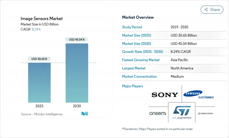
이미지 센서 시장은 2025년에 306억 5,000만 달러, 2030년에는 455억 4,000만 달러에 이르고, 예측 기간의 CAGR은 8.24%를 나타낼 전망입니다.

이 성장은 자동차 안전 의무화, 정교한 멀티 카메라 스마트폰, 반도체 수요를 재형성하는 산업 자동화 요구의 합류를 반영합니다. 자동차 제조업체는 2025년에 1대당 평균 8대의 카메라를 탑재해 2028년까지 12대의 카메라를 추가할 계획으로 센서 수량과 ASP 확대를 가속화하고 있습니다. CMOS 디바이스는 저소비전력 온칩 처리로 2024년 출하 대수의 93%를 차지하고, 적층형 이면 조사형(BSI) 설계는 2030년까지 연평균 복합 성장률(CAGR) 55%로 확대되어 보다 높은 다이나믹 레인지와 엣지에서의 AI 계산을 해방하고 있습니다. 4-12MP 해상도의 브래킷은 주류 소비자 및 산업용으로 화질과 비용이 균형을 이루기 때문에 32% 매출에서 우위를 차지하고 있습니다. 소니, 삼성, 옴니비전, 온세미는 지정학적 수출 규제, 300mm 웨이퍼 부족, 서브미크론 픽셀의 축소를 늦추는 열잡음 장벽 중 신규 진출기업으로부터 점유율을 지키기 위해 경쟁이 격화되고 있습니다.
onsemi의 Hyperlux AR0823AT는 SUBARU의 차세대 EyeSight 스테레오 카메라 슬롯을 획득하여 자율적인 의사 결정을 위한 ASIL-C 목표를 달성했습니다. 캐논 프로토타입 410MP 센서는 초당 3,280MP를 처리하여 최신 센서가 패시브 이미 저가 아닌 연산 플랫폼임을 보여주었습니다. 소니는 2019년부터 2030년 사이에 차량용 카메라의 노드 수가 6.68배로 급증할 것으로 예측하고 있으며, 높은 다이나믹 레인지, 저지연 부품에 대한 OEM의 지속적인 인계를 강조하고 있습니다. HDR, LED 플리커 완화, 기능 안전 IP는 현재 표준으로 장착되어 있으며 차량용 이미 저는 중요한 안전 인프라로 자리 잡고 있습니다.
아시아 휴대폰 생태계는 픽셀 아키텍처의 혁신을 계속 추진하고 있습니다. 삼성은 2025년부터 화성 라인을 적층 CIS 제조로 전환해 프리미엄 아이폰의 디자인 승리를 쫓고 있습니다. 이 3층 센서는 포토다이오드, 전송, 로직의 각 층을 분할하여 실적를 축소하면서 다이나믹 레인지를 향상시킵니다. 옴니비전의 OV50X는 1.6µm 픽셀로 110dB의 단일 노출 HDR을 실현하여 아시아 공급업체가 저조도 연산 이미징으로 선도하고 있음을 입증합니다. 메가픽셀 경쟁에서 화질로의 전환은 고급 BSI와 AI ISP의 통합이 사용자 경험을 차별화하는 성숙한 스마트폰 사이클을 강조합니다.
SEMI는 2024년 월산 3,000만장의 웨이퍼 생산능력을 기록하고 있지만, 생산은 아시아의 소수 주조공장에 집중하여 수요 급증시 공급 부족을 증폭시키고 있습니다. 이미지 센서 라인은 현재 동일한 300mm 도구를 둘러싸고 수익률이 높은 AI 가속기와 경쟁하고 있으며 다이 가격이 상승하고 리드 타임이 길어지고 있습니다. McKinsee에 따르면, 리소그래피에 필요한 특수 화학제품의 60%는 미국 내에서 공급되지 않으며 업스트림 위험이 증가하고 있습니다. 애리조나와 유럽 공장이 2026년 이후 양산 체제에 들어갈 때까지 가격 변동은 이미지 센서 시장 전체의 마진을 압박할 것으로 보입니다.
CMOS 센서는 2024년 출하량의 93%를 차지하며 저전력 로직 통합과 웨이퍼당 경제성을 뒷받침하고 있습니다. CMOS의 이미지 센서 시장 규모는 2025년에 287억 달러에 달하고, CCD의 수익을 능가합니다. 열 병렬 ADC와 이면 배선은 다이 면적을 축소하면서 프레임 레이트를 향상시키고, 벤더는 휴대폰 전용으로도 연간 50억-70억개의 부품을 출하하고 있습니다. 과학기기나 의료기기에서는 초저암전류를 실현하는 CCD의 발주가 계속되고 있지만, 공장투자는 CMOS로 향하는 경향이 있어 CCD의 점유율은 확실히 상승하고 있습니다. 삼성의 3층 스택은 포토다이오드, 트랜스퍼 플레인, 로직 플레인을 분리함으로써 양자 효율이 향상되어 크로스토크가 감소하는 것을 실증하고 있으며, CMOS의 리더십을 확고하게 하고 있습니다.
2세대 적층 CIS는 중복성과 결함 관리를 개선하고 2030년까지 CMOS의 CAGR을 10.2%로 예측합니다. 이 기세를 통해 중국과 인도의 신규 진출기업은 성숙 노드인 65nm 플로우의 라이선스를 취득하여 차량용 서라운드 뷰용 경쟁력 있는 이미지 센서를 출시할 수 있습니다. 이미지 센서 시장은 주조 업체가 포토닉스 모듈 전용 산화막 절연막 매설 라인과 하이브리드 본딩 라인을 증설하고 있기 때문에 여전히 CMOS의 기술 혁신에 지지되고 있습니다.
적층형 BSI의 출하는 수직 통합이 2차원 스케일링 한계를 피하기 때문에 CAGR 55%로 성장하고 있습니다. 포토다이오드층과 로직층을 분리함으로써 다이를 대형화하지 않고 집광 영역을 확대할 수 있어 1.5-2EV의 감도 향상을 실현할 수 있습니다. 캐논의 410MP 적층 풀 프레임 센서는 40 병렬 레인 경유로 3,280MP/s의 판독을 실현하고 있어, 고성능의 가능성을 나타내고 있습니다. 웨이퍼 투 웨이퍼 하이브리드 본딩이 파일럿 생산에서 24/7 생산으로 이행함에 따라 제조 수율이 향상되어 스루 실리콘 비아 적층에 비해 비용을 30% 절감하고 있습니다.
이미지 센서 시장에서 적층형 BSI는 스마트폰과 차량 탑재 ADAS의 대수 증가에 힘입어 2030년까지 이미지 센서 시장 규모의 259억 달러를 차지할 것으로 예측되고 있습니다. 프론트 사이드 BSI와 기존 BSI는 비용이 지배적인 로티어 디바이스에서 계속 유효하지만, 프리미엄 제조업체는 현재 ISP 블록, SDRAM, AI 가속기를 픽셀 매트릭스 아래에 통합한 다층 스택을 중심으로 로드맵을 정비하여 시스템 인 패키지 수렴을 추진하고 있습니다.
북미는 ADAS 규정과 방어 조달이 고사양 ASP를 견인하고 있기 때문에 매출에서 가장 규모가 큰 지역 구매자로 계속되고 있습니다. 미국은 2029년부터 모든 경차에 전방 카메라를 탑재할 것을 암묵적으로 의무화하는 자동 긴급 브레이크 규칙을 최종 결정하고 롱테일 수요를 잠갔습니다. 캐나다 Tier-1 공급업체는 온타리오의 자동차 회랑에 모여 멕시코는 미국 OEM의 모듈 조립을 받아들입니다. 이 지역의 반도체 주권 추진은 TSMC의 애리조나 메가팹(1,650억 달러)에 박차를 가하고 2027년 이후에 성숙 노드 CIS 웨이퍼를 공급할 전망입니다.
유럽은 프라이버시 최초의 스마트 시티를 강조, Chips Act를 통해 edge-AI 이미지 센서에 자금을 공급, ams OSRAM의 5억 8,800만 유로의 오스트리아 확장은 자동차 라이더 및 지자체 교통 노드 모두에 공급한다고 합니다. 독일과 프랑스는 Euro-NCAP 카메라 벤치마크를 시행하여 대륙공급업체에 파급됩니다. 현지 규제에서는 얼굴 데이터의 클라우드 보존에 상한이 설정되어 있어 센서 내 암호화와 장치 상 추론을 장려하고 있습니다.
아시아태평양은 웨이퍼 생산 능력이 가장 많고 출하 성장률도 가장 높습니다. 일본 소니는 Tier1과의 제휴를 배경으로 2026년까지 자동차용 CMOS 점유율 43%를 목표로 하고 있습니다. 한국의 삼성은 스마트폰이나 AR/VR 카메라를 보충하기 위해 월 20만 웨이퍼의 CIS 생산 능력 증강을 위해 화성을 재정비하고 있습니다. 중국은 Jilin-1 별자리의 원격 센싱 수요를 늘리지만 선진 28nm CIS 노드의 미국 수출 규제에 직면해 국내 주조는 성숙 프로세스에 대한 투자를 가속화시킵니다. 인도는 자동차 대시캠과 저가형 휴대전화의 소비 주도형 시장으로 부상하고, 이스라엘은 GaAs Fab에서 틈새 방어용 이미저를 개발하여 지역의 다양성을 확대하고 있습니다.
The image sensor market reached USD 30.65 billion in 2025 and is projected to expand to USD 45.54 billion by 2030, translating to an 8.24% CAGR over the forecast period.
Growth reflects a confluence of automotive safety mandates, sophisticated multi-camera smartphones, and industrial automation needs that are reshaping semiconductor demand. Vehicle makers are equipping an average of 8 cameras per car in 2025 and plan to add 12 cameras by 2028, accelerating sensor volumes and ASP expansion. CMOS devices capture 93% of 2024 unit shipments because of low-power on-chip processing, while stacked back-side-illuminated (BSI) designs, scaling at a 55% CAGR to 2030, unlock higher dynamic range and AI computation at the edge. The 4-12 MP resolution bracket dominates with 32% revenue because it balances image quality and cost for mainstream consumer and industrial use. Competitive intensity is rising as Sony, Samsung, OmniVision and onsemi defend share against new entrants amid geopolitical export controls, 300 mm wafer scarcity, and thermal-noise barriers that slow sub-micron pixel shrink.
Automotive safety regulation is shifting cameras from premium options to mandated equipment, transforming the image sensor market. onsemi's Hyperlux AR0823AT won Subaru's next-gen EyeSight stereo-camera slot, meeting ASIL-C targets for autonomous decision making. Canon's prototype 410 MP sensor processes 3,280 MP/s, showing that modern sensors are computational platforms, not passive imagers. Sony projects a 6.68-fold jump in car camera nodes between 2019 and 2030, highlighting sustained OEM pull for high-dynamic-range, low-latency parts. HDR, LED-flicker mitigation and functional-safety IP now come standard, positioning automotive imagers as critical safety infrastructure.
Asia's handset ecosystem keeps driving pixel-architecture breakthroughs. Samsung converted its Hwaseong line to stacked CIS fabrication starting 2025, chasing premium iPhone design wins. Its 3-layer sensor splits photodiode, transfer and logic strata, boosting dynamic range while shrinking footprint. OmniVision's OV50X delivers 110 dB single-exposure HDR with 1.6 µm pixels, proving Asian suppliers now lead in low-light computational imaging. The shift from megapixel race to image quality underscores a mature smartphone cycle where advanced BSI and AI ISP integration differentiate user experience.
SEMI records 30 million wafers-per-month capacity in 2024, yet production clusters around a handful of Asian foundries, amplifying shortages during demand spikes. Image sensor lines now compete with high-margin AI accelerators for the same 300 mm tools, lifting die prices and lengthening lead times. McKinsey observes that 60% of specialty chemicals needed for lithography lack local US supply, adding upstream risk. Until Arizona and European fabs reach volume after 2026, price swings will compress margins across the image sensor market.
Other drivers and restraints analyzed in the detailed report include:
For complete list of drivers and restraints, kindly check the Table Of Contents.
CMOS sensors owned 93% of unit shipments in 2024, underscoring their low-power logic integration and per-wafer economics. The image sensor market size for CMOS reached USD 28.7 billion in 2025, dwarfing CCD revenues. Column-parallel ADC and backside wiring lift frame rate while shrinking die area, letting vendors ship 5-7 billion parts yearly for phones alone. Scientific and medical instruments continue ordering CCDs for ultra-low dark current, yet fab investments trend to CMOS, ensuring its share rises. Samsung's 3-layer stack demonstrates how separating photodiode, transfer and logic planes lifts quantum efficiency and reduces crosstalk, cementing CMOS leadership.
Second-generation stacked CIS improves redundancy and defect management, driving a projected 10.2% unit CAGR for CMOS through 2030. This momentum allows new entrants from China and India to license mature-node 65 nm flows and still launch competitive imagers for automotive surround-view. The image sensor market remains anchored on CMOS innovation as foundries add buried oxide isolation and hybrid bonding lines dedicated to photonics modules.
Stacked BSI shipments are growing at 55% CAGR because vertical integration circumvents 2-D scaling limits. Separating photodiode and logic layers permits larger light-collection areas without enlarging die, yielding 1.5-2 EV sensitivity uplift. Canon's 410 MP stacked full-frame sensor reads 3,280 MP/s via 40 parallel lanes, showing high-performance potential. Manufacturing yields have risen as wafer-to-wafer hybrid bonding moves from pilot to 24/7 production, cutting cost by 30% versus through-silicon-via stacking.
Within the image sensor market, stacked BSI is forecast to command USD 25.9 billion of image sensor market size by 2030, underpinned by smartphone and automotive ADAS volume ramps. Front-side and conventional BSI remain viable in low-tier devices where cost dominates, but premium makers now align roadmaps around multi-layer stacks that embed ISP blocks, SDRAM and AI accelerators under the pixel matrix, driving system-in-package convergence.
The Image Sensor Market Report is Segmented by Type (CMOS, CCD), Processing Technology (Front-Side Illuminated, Back-Side Illuminated, and More), Shutter Type (Rolling, Global), Spectrum (Visible, Near-Infrared, and More), Resolution (Less Than1 MP, 1-3 MP, and More), End-User Industry (Consumer Electronics, Automotive, Industrial, and More), and Geography. The Market Forecasts are Provided in Terms of Value (USD).
North America remains the largest regional buyer measured in revenue because ADAS regulations and defense procurements drive high-spec ASP. The United States finalized automatic emergency braking rules that implicitly require forward-facing cameras in all light vehicles from 2029, locking long-tail demand. Canada's Tier-1 suppliers cluster around Ontario's automotive corridor, and Mexico hosts module assembly for US OEMs. The region's push for semiconductor sovereignty spurred TSMC's USD 165 billion Arizona megafab, anticipated to supply mature-node CIS wafers post-2027.
Europe emphasizes privacy-first smart cities, funding edge-AI image sensors via the Chips Act. ams OSRAM's EUR 588 million Austrian expansion will feed both automotive lidar and municipal traffic nodes. Germany and France enforce Euro-NCAP camera benchmarks that trickle to suppliers across the continent. Local regulations cap cloud storage of facial data, encouraging in-sensor encryption and on-device inference, cultivating a premium for secure image sensor market designs.
Asia-Pacific houses most wafer capacity and posts the fastest shipment growth. Japan's Sony aims for 43% automotive CMOS share by 2026 on the back of Tier-1 alliances. South Korea's Samsung is retooling Hwaseong for additional 200,000 wafers-per-month CIS output to backfill smartphone and AR/VR cameras. China increases remote-sensing demand for its Jilin-1 constellation yet faces US export controls on advanced 28 nm CIS nodes, prompting domestic foundries to accelerate mature-process investments. India emerges as a consumption-driven market for automotive dash-cams and low-cost phones, while Israel develops niche defense imagers in GaAs fabs, extending regional diversity.