반도체 프론트엔드 장비 시장 : 시장 점유율 분석, 산업 동향 및 통계, 성장 예측(2025-2030년)
Semiconductor Front End Equipment - Market Share Analysis, Industry Trends & Statistics, Growth Forecasts (2025 - 2030)
상품코드:1692440
리서치사:Mordor Intelligence
발행일:2025년 03월
페이지 정보:영문
라이선스 & 가격 (부가세 별도)
ㅁ Add-on 가능: 고객의 요청에 따라 일정한 범위 내에서 Customization이 가능합니다. 자세한 사항은 문의해 주시기 바랍니다.
ㅁ 보고서에 따라 최신 정보로 업데이트하여 보내드립니다. 배송기일은 문의해 주시기 바랍니다.
한글목차
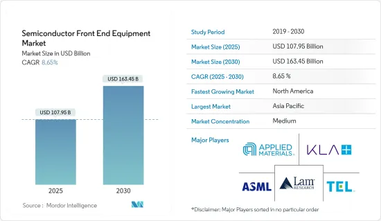
반도체 프론트엔드 장비 시장 규모는 2025년에 1,079억 5,000만 달러로 추정되고, 2030년에는 1,634억 5,000만 달러에 이를 것으로 예측되며, 예측 기간인 2025-2030년 CAGR 8.65%로 전망됩니다.
이전 단계에서는 웨이퍼를 완성된 디바이스로 변환하기 위해 많은 복잡한 단계가 필요합니다. 이러한 단계에는 웨이퍼의 세정, 산화, 디바이스를 패턴화하는 포토리소그래피, 에칭, 증착, 도핑, 메타라이제이션 등의 단계가 포함됩니다. 공정 관리에는, 검사 및 계측 장치가 이용됩니다. 이것은 최종 제품에 문제를 일으킬 가능성이 있는 불규칙성을 특정하기 위해 웨이퍼를 검사하는 것입니다. 이에 더해 광학 기술도 사용되어 미소한 결함을 찾기 위해 전자빔 검사가 필요한 경우도 많습니다.
주요 하이라이트
반도체 프론트엔드 장비 수요는 주요 전 공정 장비 제조업체가 반도체 업계의 침체를 배경으로 기록적인 수익을 달성했기 때문에 단기적인 조정이 아니라 현저한 급증이 예상됩니다. 이는 생산능력 확대, 새로운 공장 프로젝트, 그리고 전 공정 장치 시장 전체의 첨단 기술과 솔루션에 대한 높은 수요가 원동력이 되고 있습니다.
지난해, 대폭적인 매출을 기록한 웨이퍼 처리 장치, 팹 설비, 마스크 레티클 장치를 포함한 웨이퍼 제조 장치는 2023년에는 약간 저수준이 될 것으로 예측되고 있어 이번 축소는 대폭적인 개선을 의미합니다. 이번 상향 조정은 주로 중국의 호조된 설비 투자에 의한 것입니다. 시장은 미국과 네덜란드 정부의 수출 관리 규제를 포함한 지정학적 과제 및 인플레이션, 금리 상승, 특정 경제권의 GDP 성장률 저하를 둘러싼 세계 거시 우려로 인해 생긴 불확실성을 관리하며 성장했습니다.
소비자용 전자 기기가 가장 급성장하고 있는 분야이며, 시장 확대에 기여하고 있습니다. 인구 증가에 따라 증가할 것으로 예상되는 스마트폰 이용이 이 시장의 주요 촉진 요인입니다. 태블릿, 스마트폰, 노트북, PC, 웨어러블 디바이스 등의 수요 증가로 소비자용 전자기기가 업계를 견인하고 있습니다. 반도체의 진보에 따라, 기계 학습등의 새로운 시장 분야가 급속히 통합되고 있습니다.
인공지능, 사물인터넷, 양자컴퓨팅, 강화된 무선네트워크 등 미래의 가장 매력적인 '필승' 기술은 현재 반도체에 의해 지원되고 있습니다. 반도체와 마이크로일렉트로닉스는 세계가 획기적인 기술을 삶의 모든 측면에 매끄럽게 통합하는 가운데 끊임없이 변화하는 디지털 환경의 복잡한 요구를 충족시키기 위해 진보하고 있습니다. 빅데이터와 AI가 이러한 증가를 뒷받침하고 더 작고 강력한 칩을 요구하고 있기 때문에 그 제조는 더 어려워지고 기술 혁신의 필요성이 커지고 있습니다.
데이터 스토리지, 계산 능력, 알고리즘의 급속한 진보에 의해 AI 시스템의 개발과 전개가 가능하게 되었습니다. 디지털 기기와 인터넷의 이용이 증가함에 따라 대량의 데이터가 생성되게 되었습니다. AI 시스템은 학습과 성능 향상을 위해 대규모 데이터 세트에 의존하고 있습니다.
사물인터넷(IoT), 빅데이터, 클라우드 매뉴팩처링, 사이버피지컬시스템(CPS), 서비스인터넷(IoS), 로봇공학, 증강현실(AR), 기타 신흥기술은 인더스트리 4.0의 개녑에 포함되어 있습니다. 새로운 스마트한 산업 프로세스를 만들기 위해서는 이러한 기술을 채택하는 것이 중요하며, 그것은 미래 산업의 진보를 몇 가지 포함함으로써 물리적인 세계와 디지털 세계를 통합하게 됩니다.
세계 재택 근무 동향이 증가함에 따라 클라우드 서비스에 대한 수요가 급증하고 데이터센터 공급자는 그 능력을 확장해야 할 필요가 있습니다. 그 결과, 칩과 메모리에 대한 세계의 수요가 높아집니다. SEMI는 300mm 팹에 대한 투자가 현저히 증가하고 있다고 보고하고 있습니다. 예측에 따르면 업계에서는 2020-2024년 최소 38개의 300mm 팹이 신설됩니다.
이 급증에 따라 웨이퍼 생산 능력은 약 180만 장 증가해 합계로 700만 장을 넘게 됩니다. 주목할 만한 것은 대만이 이 중 11곳의 새로운 양산 공장을 건설할 예정이고, 중국이 8곳에서 이를 뒤따른다는 점입니다. 게다가 TSMC는 애리조나에 새로운 300mm 팹을 건설 중입니다. 2024년 말까지 300mm 양산 공장은 161개에 이를 것으로 예상됩니다.
반도체 프론트엔드 장비 시장 동향
반도체 제조 공장이 가장 큰 최종 사용자 산업으로
설계 단계 후, 반도체 칩은 팹이나 주조라고 불리는 시설에서 제조됩니다. 프론트 엔드 패브리케이션에서 칩은 웨이퍼라고 불리는 실리콘 원형 시트 또는 덜 일반적인 다른 반도체 재료 위에 제조됩니다.
패브리케이션은 다양한 중소기업과 재료에 따라 설계를 칩으로 바꾸는 프로세스입니다. 먼저 용광로에서 실리콘의 원주를 형성하고 그것을 원반 모양의 웨이퍼로 절단합니다. 반도체 제조시설('팹')은 실리콘 내의 재료층에 트랜지스터나 기타 전기 디바이스를 형성하고, 실리콘 위의 절연층에 전기 디바이스간의 금속 상호 접속을 형성한다고 하는 2개의 스텝으로 칩을 웨이퍼로 만듭니다. 전기 장치와 상호 연결이 결합되어 회로가 형성됩니다.
미국, 대만, 한국, 일본, 중국에 본사를 두는 기업이 세계 반도체 제조 공장 시장 점유율과 제조 능력의 대부분을 지배하고 있으며, 이들 기업은 물리적으로도 이들 국가에 위치하고 있습니다. 반도체 제품의 개발에는, (재료로부터 물류에 이르기까지) 많은 비즈니스가 조화롭게 일하는 것이 필요합니다. 반도체 디바이스의 제조 공정이 복잡하기 때문에 개발 비용도 증대하고 있습니다. 기업은 다양한 비즈니스 모델을 활용함으로써 지출을 줄이고 반도체에서 생존을 도모해 왔습니다.
2023년 11월, 중국은 8억 1,680만 달러에 해당하는 42대의 리소그래피 시스템을 가져왔습니다. 네덜란드는 16대의 리소그래피 시스템을 공급했으며, 총액은 7억 6,270만 달러로 전년보다 10배 증가했습니다. 게다가 중국은 10월에 네덜란드에서 21대의 시스템을 수입했습니다. 일본의 캐논과 니콘도 중국에 노광 장치를 공급했습니다. 이와 같이 반도체 제조 공장에서의 전공정 장치 수요는 상향 조정이 예상됩니다.
세계 경제의 회복이 예상되어 내년 스마트폰, 서버, 노트북, TV, 자동차 시장의 성장뿐만 아니라 5G 기지국과 Wi-Fi 6 기술을 포함한 차세대 네트워크의 지속적인 전개에 의해 부품 수요 증가가 예상됩니다.
European 5G Observatory에 따르면 2023년 시점에서 독일은 유럽연합(EU) 회원국 중 최대 5G 기지국을 가지고 있으며, 약 9만 기지국이 설치되어 있습니다. 이러한 칩의 설계 및 제조와 그 연구는, 수십만개의 고임금의 고용을 제공할 수 있기 때문에, 온쇼어링 및 리쇼어링은 정치적으로 인기있는 화제가 되고 있습니다. 따라서 주조소와 장치 제조업체는 각각의 백야드에서 막대한 투자를 계획하고 매핑하고 있습니다. 예를 들어 도쿄 일렉트론은 일본의 장치 제조 설비에 6억 달러 이상을 투자할 계획을 발표했습니다.
IDM은 웨이퍼 제조 능력에 투자함으로써 여전히 중요한 역할을 하고 있습니다. 예를 들어 2023년 6월 인텔과 독일 정부는 마그데부르크에 300억 유로 이상의 최첨단 웨이퍼 제조 거점을 계획하기 위한 수정 취지서에 서명하고 2개의 유럽 최초 반도체 시설을 건설하겠다고 발표했습니다. 한국 언론에 따르면 이 회사는 2023년 12월 ASML로부터 고NA의 EUV 노광 장치 6대를 취득해 2024년에 출하할 예정이라고 보도되고 있습니다. 이 인수는 2nm 노드에서 삼성이나 TSMC를 앞지르기 위한 비밀병기가 될 것으로 보입니다.
2023년 7월, 삼성은 텍사스주 오스틴의 1,200에이커의 토지에 170억 달러를 투입해 반도체 제조 공장을 건설한다고 발표했습니다. 중국과 대만 간의 지정학적 긴장 때문에 칩 제조업체는 미국에 제조 거점을 요청했습니다. 세금이 저렴하고 새로운 보조금도 있기 때문에 텍사스는 사업을 하기에 적합한 장소로 떠올랐습니다. 세계 반도체 제조 장치 업체들은 한국에서 시설을 확장하고 있습니다. 새로운 국내 생산 거점에 향후 20년간에 2,300억 달러를 투자할 계획으로, 다른 기업을 끌어들여 칩 공급 체제를 육성하고 있습니다.
중국이 큰 시장 점유율을 차지할 전망
CSET에 따르면 중국은 조립 및 패키징 툴을 제외한 모든 주요 부문에서 주목할만한 시장 점유율을 차지하고 있습니다. 그러나 리소그래피 장치, 특히 극단자외선(EUV) 포토리소그래피와 심자외선(DUV) 포토리소그래피에서 중국은 최대 과제에 직면해 있습니다.
임프린트 리소그래피, 전자빔, 레이저 리소그래피, 레지스트 처리 장치, 포토마스크 검사, 리페어 툴 등이 큰 장해가 되고 있습니다. 지난 몇 년간 중국은 칩 산업을 지탱하기 위해 선진적인 리소그래피 장치 수입에 일관되게 투자해 왔습니다.
그러나, 그 기술력을 배경으로, 중국은 항상 전 공정 장치에의 의존도를 높여, 그것을 시장에 도입하기 위해 대규모 투자를 실시했습니다.
2023년 12월, 중국의 리소그래피 장치 전문 기업인 상하이 미전자 설비 집단(SMEE)은 28nm 클래스의 최첨단 프로세스 기술로 웨이퍼 가공이 가능한 초호기를 발표했습니다. 이 중요한 성과는 SMEE의 선진적인 리소그래피 장치 구축에 대한 헌신을 부각시키는 것입니다. 이 장치는 SSA/800-10W라고 불리며, 동사에 있어서 중요한 이정표가 됩니다.
미국의 제재 조치는 일중 간 기술적 대립이 격화하는 가운데 세계적으로 최첨단 칩을 개발하는 중국의 진보를 방해하기 위해 책정되었습니다. SMIC와 다른 칩 메이커는, 칩 생산을 진행하는 것으로 국가의 자주성을 높이는 것에 전념하고 있습니다. SMIC는 선진적인 리소그래피 장치를 활용해 현지 장치 업체들과 긴밀히 협력하고 첨단 노드 프로세스의 수율을 높이기 위해 화웨이에 외부 지원을 요청하고 있습니다.
미국의 중국 기술에 대한 제재가 계속되고 있기 때문에 이 지역은 자급 자족에 노력하고 있습니다. 중국 정부는 첨단 칩 기술의 연구 개발에 다액의 투자를 실시했습니다. 또, 경제나 전기 자동차(EV)와 같은 신흥 산업에서 다양한 용도로 사용되는 고노드 칩에 중점을 옮기도록, 현지 제조업체를 장려하고 있습니다. 정부의 이니셔티브 고조 및 국내 칩 생산을 강화하기 위한 현지 벤더에 의한 투자의 증가는 프론트 엔드 시장에 주목할 만한 수요를 창출할 것으로 예상됩니다.
CAAM에 따르면 2023년 8월 중국의 신에너지차 판매 대수는 약 84만 6,000대로 80만 8,000대가 승용 전기자동차, 3만 9,000대가 상용 전기자동차였습니다. 승용 배터리 전기차(BEV)는 55.9만 대, 승용 플러그인 하이브리드 전기차(PHEV)는 24.8만 대였습니다.
반도체 프론트엔드 장비 시장 개요
반도체 프런트엔드 장비 시장은 Applied Materials Inc., ASML Holding NV, Tokyo Electron Limited, LAM Research Corporation, KLA Corporation과 같은 주요 업체들이 반쯤 통합되어 있습니다. 시장 참여자들은 제품 제공을 강화하고 지속 가능한 경쟁 우위를 확보하기 위해 파트너십, 혁신, 인수 등의 전략을 채택하고 있습니다.
2024년 2월-ASML Holding NV는 에어버스 A320형기 2기분의 무게를 가지는 가격 3억 5,000만 유로의 최신 칩 제조기 'High-NA'를 발표했습니다. 인텔은 오리건 공장에 첫 출하를 확보했으며 칩 생산은 내년 후반에 시작될 예정입니다. 이 비행기는 8나노미터 두께의 반도체 라인을 실현해, 종래의 1.7배로 축소, 칩의 트랜지스터 밀도를 높여 처리 속도와 메모리를 향상시킵니다.
2024년 1월-어플라이드 머티리얼즈가 구글과 제휴해 증강현실(AR) 기술을 추진했습니다. 이 제휴는 어플라이드 머티리얼즈의 재료공학 전문지식과 구글의 플랫폼을 활용하여 차세대 AR 체험을 위한 경량 비주얼 디스플레이 시스템을 개발하는 것입니다. 그 목적은 여러 세대의 AR 제품, 애플리케이션, 서비스 개발을 가속화하는 것입니다.
기타 혜택
엑셀 형식 시장 예측(ME) 시트
3개월간의 애널리스트 서포트
목차
제1장 서론
조사의 전제조건 및 시장 정의
조사 범위
제2장 조사 방법
제3장 주요 요약
제4장 시장 인사이트
시장 개요
업계의 매력도-Porter's Five Forces 분석
공급기업의 협상력
구매자의 협상력
신규 참가업체의 위협
대체품의 위협
경쟁도
업계 밸류체인 분석
COVID-19 팬데믹 시장에 대한 영향
제5장 시장 역학
시장 성장 촉진요인
소비자용 전자 기기에 대한 요구 고조가 제조업 전망을 촉진
업계별 인공지능, IoT, 커넥티드 디바이스의 보급
시장 성장 억제요인
기술의 다이나믹한 성질에 의해 제조 설비에 수회의 변경 필요
제6장 시장 세분화
유형별
리소그래피 장치
에칭 장비
증착 장치
기타 장치 유형
최종 사용자 산업별
반도체 제조 공장
반도체 일렉트로닉스 제조
지역별
미국
유럽
중국
한국
대만
일본
라틴아메리카
중동 및 아프리카
제7장 경쟁 구도
기업 프로파일
Applied Materials Inc.
ASML Holding NV
Tokyo Electron Limited
LAM Research Corporation
KLA Corporation
Nikon Corporation
VEECO Instruments Inc.
Plasma Therm
Hitachi High-Technologies Corporation
Carl Zeiss AG
Screen Holdings Co. Ltd
제8장 투자 분석
제9장 시장의 미래
AJY
영문 목차
영문목차
The Semiconductor Front End Equipment Market size is estimated at USD 107.95 billion in 2025, and is expected to reach USD 163.45 billion by 2030, at a CAGR of 8.65% during the forecast period (2025-2030).
The front-end procedure necessitates a multitude of intricate phases to convert a wafer into a completed device. These steps incorporate wafer cleaning, oxidation, and photolithography to pattern devices, along with etching, deposition, doping, and metallization steps. Inspection and metrology equipment is utilized for process control. This is when the wafers are inspected to identify irregularities that potentially induce issues with the end product. In addition to this, optical techniques are also used, and e-beam inspection is often needed to find the smallest defects.
Key Highlights
The demand for semiconductor front-end equipment is expected to observe a noteworthy surge as some of the major front-end equipment-producing companies observed record-breaking revenue against a backdrop of a downturn in the semiconductor industry instead of the mild and short-term correction. It was driven by capacity expansion, new fab projects, and high demand for advanced technologies and solutions across the front-end equipment market.
After registering a record of significant sales last year, the wafer fab equipment, which includes wafer processing, fab facilities, and mask/reticle equipment, is projected to be a bit low in 2023, and this contraction marks a significant improvement. The upward revision is primarily due to China's strong equipment spending. The market grew managing uncertainties created by geopolitical challenges, including the US and Dutch governments' export control regulations and global macro concerns around inflation, rising interest rates, and lower GDP growth in certain economies.
Consumer electronics is the fastest-growing segment, contributing to market expansion. The use of smartphones, anticipated to rise with population growth, is the key driver of this market. Consumer electronics drive the industry due to increased demand for tablets, smartphones, laptops, computers, and wearable gadgets. As semiconductors advance, new market areas, such as machine learning, are rapidly being integrated.
The most fascinating "must-win" technologies of the future, such as artificial intelligence, the Internet of Things, quantum computing, and enhanced wireless networks, are currently supported by semiconductors. Semiconductors and microelectronics are advancing to satisfy the complicated demands of a constantly changing digital environment as the world seamlessly integrates breakthrough technology into every aspect of life. Big Data and AI drive this increase and call for smaller, more powerful chips, making their production more difficult and increasing the need for technological innovation.
Rapid advancements in data storage, computing power, and algorithms have enabled the development and deployment of AI systems. The increased use of digital devices and the Internet has generated extensive volumes of data. AI systems rely on large datasets to train and improve their performance.
The Internet of Things (IoT), big data, cloud manufacturing, cyber-physical systems (CPS), the Internet of Services (IoS), robotics, augmented reality, and other emerging technologies are included in the Industry 4.0 idea. Creating additional smart industrial processes depends on adopting these technologies, which will unite the physical and digital worlds by encompassing several future industrial advancements.
As global work-from-home trends gain momentum, the demand for cloud services surges, prompting data center providers to expand their capacities. This, in turn, fuels the global appetite for chips and memory. SEMI reports a notable uptick in investments in 300 mm fabs. Projections suggest that the industry will witness the addition of a minimum of 38 new 300 mm fabs between 2020 and 2024.
This surge is set to boost the capacity by approximately 1.8 million wafers, pushing the total beyond 7 million. Notably, Taiwan is slated to host 11 of these new volume fabs, with China following closely with eight. Additionally, TSMC is in the process of constructing a new 300 mm fab in Arizona. By the close of 2024, the tally of 300 mm volume fabs is anticipated to hit a significant 161 units.
Semiconductor Front End Equipment Market Trends
Semiconductor Fabrication Plant to be the Largest End-user Industry
After the design stage, semiconductor chips are manufactured or fabricated in facilities called fabs or foundries. In front-end fabrication, chips are manufactured on circular sheets of silicon or, less commonly, other semiconducting materials called wafers, typically about 8 or 12 inches in diameter.
Fabrication is a process that turns designs into chips, relying on various SMEs and materials. First, a furnace forms a cylinder of silicon, which is cut into disc-shaped wafers. Semiconductor fabrication facilities ("fabs") make chips into wafers in two steps: forming transistors and other electrical devices in material layers within the silicon and forming metal interconnects between the electrical devices in insulating layers above the silicon. Together, the electrical devices and interconnects form circuits.
Firms headquartered in the United States, Taiwan, South Korea, Japan, and China control most of the world's fab market share and fab capacity, which are also physically located in these countries. Semiconductor product development requires working harmoniously for many businesses (from materials to logistics). The complex process of fabricating semiconductor devices has also increased the development cost. Companies have leveraged different business models to lower expenditures and survive in semiconductors.
In November 2023, China brought 42 lithography systems worth USD 816.8 million. The Netherlands supplied 16 lithography systems, totaling USD 762.7 million, a tenfold increase from the previous year. Additionally, China imported 21 systems from the Netherlands in October. Japanese companies Canon and Nikon also supplied China with lithography tools. Thus, an upward revision is expected in the demand for front-end equipment in semiconductor fabrication plants.
The global economy is expected to recover, and the demand for components is expected to rise owing to not only growth in the smartphone, server, notebook computer, TV, and automobile markets next year but also the continued rollout of next-generation networks, including 5G base stations and Wi-Fi 6 technologies.
According to the European 5G Observatory, as of 2023, Germany had the maximum 5G base stations among European Union (EU) member states, with approximately 90,000 base stations installed. The design and manufacturing of these chips and their research can provide hundreds of thousands of high-paying jobs, making onshoring/re-shoring a popular topic politically. It is why foundries and equipment companies are planning and mapping enormous investments in their backyards. For instance, TEL announced plans to invest more than USD 600 million in equipment manufacturing facilities in Japan.
IDMs still play a significant role by investing in wafer fabrication capacities. For instance, in June 2023, Intel and the German government announced signing a revised letter of intent for planning a leading-edge wafer fabrication site in Magdeburg with more than EUR 30 billion for two first-of-a-kind European semiconductor facilities. In December 2023, the company reportedly acquired six high-NA EUV lithography machines from ASML, which is scheduled for shipment in 2024, according to South Korean media outlets. This acquisition is expected to be its secret weapon to overtake Samsung and TSMC at the 2nm node.
In July 2023, Samsung announced it would spend USD 17 billion to build a semiconductor fabrication plant on a 1,200-acre plot of land in Austin, Texas. Owing to the geopolitical tension between China and Taiwan, chipmakers turned to the United States for manufacturing. Due to low taxes and new subsidies, Texas has emerged as a suitable place to do business. Global semiconductor manufacturing equipment companies are expanding facilities in South Korea. The company plans to invest USD 230 billion over the next 20 years in a new domestic production hub, attracting other players and fostering a chip supply system.
China is Expected to Hold a Significant Market Share
According to CSET, China holds a noteworthy market share in all major segments besides assembly and packaging tools. However, China faces the greatest challenge in lithography tools, particularly extreme ultraviolet (EUV) photolithography and deep ultraviolet (DUV) photolithography.
Imprint lithography, e-beam, laser lithography, resist processing equipment, photomask inspection, and repair tools pose significant obstacles. Over the past few years, China has consistently invested in importing advanced lithography equipment to support its chip industry.
However, with its technological capabilities, the country constantly strives to enhance its self-dependency on front-end equipment and invest significantly to introduce it into the market.
In December 2023, Shanghai Micro Electronics Equipment Group (SMEE), a Chinese company specializing in lithography tools, unveiled its inaugural machine capable of processing wafers using a cutting-edge 28nm-class process technology. This significant achievement highlights SMEE's dedication to constructing advanced lithography machines. The scanner, known as SSA/800-10W, marks a significant milestone for the company.
US sanctions have been formulated to impede China's progress in developing the most cutting-edge chips globally as the technological rivalry between the two countries intensifies. SMIC and other chip manufacturers are dedicated to enhancing the nation's autonomy by advancing chip production. SMIC collaborates closely with local tool manufacturers, utilizing its advanced lithography equipment, and seeks external assistance from Huawei to enhance yields in advanced node processes.
Due to the continuous US sanctions on Chinese technology, the area strives for self-sufficiency. The Chinese government is investing substantially in the research and development of advanced chip technology. It also encourages local manufacturers to shift their focus to higher-node chips with various uses in the economy and emerging industries like electric vehicles (EVs). The growing government initiatives and the increasing investments by local vendors to boost domestic chip production are expected to create a notable demand for the front-end market.
According to CAAM, in August 2023, China's new energy vehicle sales were approximately 846,000 units, of which 808,000 were passenger electric vehicles and 39,000 were commercial electric vehicles. The sales of passenger battery electric vehicles (BEVs) and passenger plug-in hybrid electric vehicles (PHEVs) were 559,000 and 248,000 units, respectively.
Semiconductor Front End Equipment Market Overview
The semiconductor front-end equipment market is semi-consolidated, with major players like Applied Materials Inc., ASML Holding NV, Tokyo Electron Limited, LAM Research Corporation, and KLA Corporation. Market players are adopting strategies such as partnerships, innovations, and acquisitions to enhance their product offerings and gain sustainable competitive advantage.
February 2024 - ASML Holding NV unveiled its latest chipmaking machine, the High-NA extreme ultraviolet, priced at EUR 350 million, weighing as much as two Airbus A320s. Intel Corp. secured the first shipment for its Oregon factory, with chip production set to begin late next year. The machine achieves 8-nanometer thick semiconductor lines, 1.7 times smaller than its predecessor, enhancing chip transistor density for increased processing speeds and memory.
January 2024 - Applied Materials Inc. collaborated with Google to advance augmented reality (AR) technologies. This partnership leverages Applied Materials' expertise in materials engineering with Google's platforms to develop lightweight visual display systems for the next era of AR experiences. The goal is to expedite the creation of multiple generations of AR products, applications, and services.
Additional Benefits:
The market estimate (ME) sheet in Excel format
3 months of analyst support
TABLE OF CONTENTS
1 INTRODUCTION
1.1 Study Assumptions and Market Definition
1.2 Scope of the Study
2 RESEARCH METHODOLOGY
3 EXECUTIVE SUMMARY
4 MARKET INSIGHTS
4.1 Market Overview
4.2 Industry Attractiveness - Porter's Five Forces Analysis
4.2.1 Bargaining Power of Suppliers
4.2.2 Bargaining Power of Buyers
4.2.3 Threat of New Entrants
4.2.4 Threat of Substitute Products
4.2.5 Degree of Competition
4.3 Industry Value Chain Analysis
4.4 Impact of COVID-19 Pandemic on the Market
5 MARKET DYNAMICS
5.1 Market Drivers
5.1.1 Increasing Needs of Consumer Electronic Devices Boosting the Manufacturing Prospects
5.1.2 Proliferation of Artificial Intelligence, IoT, and Connected Devices Across Industry Verticals
5.2 Market Restraints
5.2.1 Dynamic Nature of Technologies Requires Several Changes in Manufacturing Equipment