박형 웨이퍼 가공 및 다이싱 장비 시장 : 점유율 분석, 산업 동향, 성장 예측(2025-2030년)
Thin Wafer Processing And Dicing Equipment - Market Share Analysis, Industry Trends & Statistics, Growth Forecasts (2025 - 2030)
상품코드:1687405
리서치사:Mordor Intelligence
발행일:2025년 03월
페이지 정보:영문
라이선스 & 가격 (부가세 별도)
ㅁ Add-on 가능: 고객의 요청에 따라 일정한 범위 내에서 Customization이 가능합니다. 자세한 사항은 문의해 주시기 바랍니다.
ㅁ 보고서에 따라 최신 정보로 업데이트하여 보내드립니다. 배송기일은 문의해 주시기 바랍니다.
한글목차
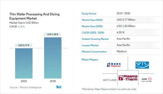
세계의 박형 웨이퍼 가공 및 다이싱 장비 시장 규모는 2025년 7억 7,000만 달러로 추정되며, 예측 기간 중(2025-2030년) CAGR 6.35%로 확대되어, 2030년에는 10억 5,000만 달러에 달할 것으로 예측되고 있습니다.
주요 하이라이트
전자 부품의 사용량 증가에 의한 막대한 수요에 의해 전자 패키징을 고도로 자원화하는 대처가 증가하고 있어, 전자 패키징은 무수한 용도로 유용하게 되고 있습니다.
향후 수년간, 박형 웨이퍼 가공 및 다이싱 장비 수요를 끌어올릴 것으로 예상되는 주요인 중 하나는 메모리 카드, 스마트폰, 스마트 카드, 각종 컴퓨팅 디바이스 등의 소형 반도체 디바이스에 널리 사용되고 있는 3차원 집적 회로에 대한 수요 증가입니다.
3차원 회로는 고속성, 내구성, 저소비 전력, 메모리의 경량화 등, 제품 전체의 성능을 향상시키기 위해, 휴대가전, 센서, MEMS, 공업 제품 등, 공간에 제약이 있는 복수의 용도으로 보급이 진행되고 있습니다.
저비용 클라우드 컴퓨팅 솔루션이 보급됨에 따라 다양한 기업과 산업에서 서버 및 데이터센터 시스템의 사용이 확대되고 있으며 마이크로프로세서 및 디지털 신호 프로세서와 같은 로직 디바이스에 대한 수요가 증가 할 수 있습니다. 하지만 높은 IoT 대응 링크 디바이스 증가에 따라 마이크로프로세서의 이용도 증가하고 있습니다.
실리콘 웨이퍼는 마이크로 일렉트로닉스 및 MEMS 제조 플랫폼으로 오랫동안 사용되어 왔습니다. 실리콘 온 인슐레이터 기판은 표준 실리콘 웨이퍼의 독특한 변형입니다. 두께 약 1-2μm의 이산화실리콘 본드층을 사용하여 2장의 웨이퍼를 접착하여 웨이퍼를 만듭니다.
최첨단 박형 웨이퍼 파운드리의 건설 비용은 지수적으로 상승해 시장을 압박하고 있습니다. 반도체 제조업체의 수는 최근 통합되어 있습니다. 성능 향상이 둔화되어, 특수한 박형 웨이퍼의 매력은 점점 더 높아지고 있습니다.
반도체 연구의 다양한 개발이 시장에 추가적인 기회를 가져왔습니다.
박형 웨이퍼 가공 및 다이싱 장비 시장 동향
반도체의 소형화 요구 증가가 시장을 견인
미국 소비자기술협회(Consumer Technology Association)에 따르면, 미국에서는 2022년부터 2024년까지 가전제품의 소매 매출이 미세 증가하고, 그 총액은 5,000억 달러 이상에 달할 것으로 예상되고 있습니다. 헬스케어나 자동차용 반도체 IC 제조업체 등 다른 최종사용자와 함께, 가전제품 수요는 IC의 소형화를 강요하고 있습니다.
지역별로는 팹리스 및 비즈니스 모델이 세계의 반도체 판매에 있어서 아시아 국가가 돌출한 지위를 차지하는 주된 요인이 되고 있습니다.
Fujifilm에 의하면 AI, IoT, 차세대 통신 규격 「5G」의 이용 확대나 자율 주행 기술의 진전에 의해 반도체 수요나 성능의 향상이 전망되기 때문에 반도체 디바이스의 미세화가 계속되고 있습니다 위와 같은 요인으로부터, 최고의 성능을 발휘하기 위해, 극박 실리콘 웨이퍼상에 구축된 3차원 회로 아키텍처에 의존하는 소형 및 경량의 소비자용 디바이스 수요가 높아지고 있습니다.
이 웨이퍼는 매우 얇고 평탄합니다. 동시에, 소형화에 의해 1개의 칩에 복수의 기능을 집적할 필요가 생기고 있습니다.
2023년 12월 Samsung Electronics와 ASML Holding NV는 한국에 선진적인 연구개발(R&D) 시설을 설립하기 위해 7억 6,000만 달러를 공동으로 투자한다고 발표했습니다. 특히 ASML의 최첨단 EUV 기술의 활용에 중점을 두고 있습니다.
아시아태평양이 가장 큰 시장 점유율을 차지할 전망
아시아태평양은 세계 최대이고 가장 급성장하고 있는 반도체 시장입니다.
중국의 다양한 시장 기업은 인수와 합병을 통해 사업을 확대하는 데 주력하고 있습니다. 중국의 Huatian Technology가 대부분을 소유하는 Unisem과 다른 말레이시아의 칩 패키징 기업은 중국의 파트너로부터의 비즈니스나 문의 증가가 눈에 띕니다.
세계 반도체 산업의 역학 변화를 감안할 때, 베트남이나 인도와 같은 다른 국가들도 칩 제조 서비스의 대안이 되려고 합니다.
일본은 여러 대형 제조업체와 일렉트로닉스 산업의 본거지이기 때문에 반도체 산업에 있어서 필수적인 지위를 차지하고 있습니다. 일본의 조직은 반도체 제조와 패키징에 소비되는 가장 중요한 재료의 중요한 공급자로 간주됩니다.
호주에서는 전자기기 제조업이 성장하고 있어 다양한 최종사용자 산업에서 첨단기기의 채용이 증가하고 있는 것이 시장 성장에 영향을 주고 있습니다.
2023년 12월, 시드니 대학 나노연구소는 레고 블록처럼 설계되었으며 대역폭이 개선된 새로운 칩을 발표했습니다. 이 획기적인 기술로 무선 주파수(RF)의 대역폭이 대폭 넓어져 칩 내 정보 관리의 정확도가 향상됩니다.
완전 자동운전차의 성장궤도는 기술의 진보, 완전자동운전차를 받아들이는 소비자의 의욕, 가격설정, 자동차의 안전성에 대한 중대한 우려에 대처하는 공급자와 OEM의 능력 등 아시아태평양의 요인에 크게 영향을 받습니다.
박형 웨이퍼 가공 및 다이싱 장비 산업 개요
박형 웨이퍼 가공 및 다이싱 장비 시장은 반고체화하고 있으며, Disco Corporation, Panasonic Corporation, Nippon, Pulse Motor Taiwan 등, 극히 소수의 대기업으로 구성되어 있습니다. 이 시장은 박형 웨이퍼 제조 공정에서 여전히 큰 문제에 직면하고 있습니다. 상기의 요인에 의해 신규 참가의 움직임은 둔합니다. 그럼에도 불구하고 시장의 끊임없는 기술 혁신과 R&D 노력은 경쟁력을 유지하는 데 도움이 됩니다. 따라서 시장에서 경쟁업체 간의 적대관계는 완만합니다.
2024년 3월: Hitachi High-Tech는 논패턴 웨이퍼의 앞뒤면의 파티클이나 결함을 검사하는 새로운 시스템 「LS9300AD」의 발매를 발표했습니다. LS9300AD는 기존 암시 레이저 산란법에 의한 이물 및 결함 검출에 더해, 새롭게 DIC(미분 간섭 콘트라스트) 검사 기능을 탑재해, 얕은 저어스펙트의 미세한 요철 결함도 검출할 수 있습니다. LS9300AD는 기존 제품으로 채용하고 있는 웨이퍼 엣지 그립 방식과 회전 스테이지를 채용해, 웨이퍼의 표리 검사가 가능합니다.
2023년 11월 Corning Inc.은 독일의 레이저 기술 사업을 중국의 Suzhou Delphi 레이저에 판매했습니다. 이 계약은 Corning Laser Technologies로 알려진 부문의 전체 주식을 Suzhou Delphi Laser가 취득한 것이었습니다.
기타 혜택:
엑셀 형식 시장 예측(ME) 시트
3개월간의 애널리스트 서포트
목차
제1장 서론
조사의 전제조건과 시장 정의
조사 범위
제2장 조사 방법
제3장 주요 요약
제4장 시장 인사이트
시장 개요
업계의 매력 Porter's Five Forces 분석
신규 참가업체의 위협
구매자의 협상력
공급기업의 협상력
대체품의 위협
경쟁 기업간 경쟁 관계의 강도
업계 밸류체인 분석
COVID-19의 부작용 및 기타 거시 경제 요인이 시장에 미치는 영향
제5장 시장 역학
시장 성장 촉진요인
스마트 카드, RFID 기술, 차량용 파워 IC 수요 증가
반도체의 소형화 요구 증가
시장 성장 억제요인
제조상의 과제
제6장 시장 세분화
장치 유형별
박막화 장치
다이싱 장비
블레이드 다이싱
레이저 어블레이션
스텔스 다이싱
플라즈마 다이싱
용도별
메모리 로직(TSV)
MEMS 디바이스
파워 디바이스
CMOS 이미지 센서
RFID
기타
웨이퍼 두께별
750마이크로미터
120마이크로미터
50마이크로미터
웨이퍼 사이즈별
4인치 이하
5인치 및 6인치
8인치
12인치
지역별
북미
유럽
아시아
호주 및 뉴질랜드
라틴아메리카
중동 및 아프리카
제7장 경쟁 구도
기업 프로파일
Suzhou Delphi Laser Co. Ltd
SPTS Technologies Limited
Plasma-Therm LLC
Han's Laser Technology Industry Group Co. Ltd
ASM Laser Separation International(ALSI) BV
Disco Corporation
Tokyo Seimitsu Co, Ltd(Accretech)
Neon Tech Co. Ltd
Advanced Dicing Technologies Ltd
Panasonic Corporation
Hitachi High-Tech Corporation
제8장 투자 분석
제9장 시장 기회와 앞으로의 동향
JHS
영문 목차
영문목차
The Thin Wafer Processing And Dicing Equipment Market size is estimated at USD 0.77 billion in 2025, and is expected to reach USD 1.05 billion by 2030, at a CAGR of 6.35% during the forecast period (2025-2030).
Key Highlights
The increasing efforts to make electronic packaging highly resourceful due to the enormous demand for electronic components owing to amplified usage have made electronic packaging useful in a myriad of applications. These factors are driving the growth of the semiconductor and IC packaging market.
One of the major factors expected to boost the demand for thin wafer processing and dicing equipment in the coming years is the growing demand for three-dimensional integrated circuits, which are widely used in miniature semiconductor devices such as memory cards, smartphones, smart cards, and various computing devices.
Three-dimensional circuits are becoming more popular in multiple space-constrained applications, such as portable consumer electronics, sensors, MEMS, and industrial products because they improve overall product performance in terms of speed, durability, low power consumption, and lightweight memory.
Due to the widespread availability of low-cost cloud computing solutions, the expanding use of server and data center systems across various enterprises and industries is likely to fuel demand for logic devices like microprocessors and digital signal processors. In addition, as the number of IoT-enabled linked devices grows, the utilization of microprocessors also increases. Thin wafers are increasingly employed in these devices to enable effective temperature management and enhance performance. Such factors are responsible for the growth of the market.
Silicon wafers have long been used as a fabrication platform in microelectronics and MEMS. The silicon-on-insulator substrate is a unique variation of the standard silicon wafer. Two silicon wafers are glued together using a bond layer of silicon dioxide with a thickness of about 1-2 μm to make these wafers. One silicon wafer gets flattened down to 10-50 μm in thickness. The application will determine the exact thickness of the coating.
The cost of building state-of-the-art thin wafer foundries has increased exponentially, which puts pressure on the market. The number of semiconductor manufacturers has consolidated in recent times. Performance boosts are slowing down, making specialized thin wafers increasingly attractive. The design decisions that enable thin wafers to be universal may be sub-optimal for some computing tasks.
Various developments in semiconductor research further create opportunities for the market. For instance, in April 2023, Rapidus officially joined Imec's Core Partner Program, marking a significant stride in sustainable collaboration with Imec in advanced semiconductor research. This move reinforced their commitment to long-term collaboration and advancement in the semiconductor domain.
Thin Wafer Processing And Dicing Equipment Market Trends
Increasing Need for Miniaturization of Semiconductors is Expected to Drive the Market
According to the Consumer Technology Association, in the US, retail sales of consumer electronics were expected to grow marginally between 2022 and 2024, with the total value exceeding USD 500 billion. This would increase the demand for wafers to develop electronic products. The demand for consumer electronics products, along with other end users such as healthcare and automotive semiconductor IC manufacturers, is forcing them to reduce the size of ICs. It has, therefore, given rise to miniaturization in the market, which is expected to experience a surge in its demand during the forecast period.
Across geographies, the fabless business model is the major contributor to the prominent position of various Asian countries in semiconductor sales worldwide. Fabless firms typically outsource fabrication to pure-play foundries and outsourced assembly and test (OSAT) firms.
According to Fujifilm, the miniaturization of semiconductor devices continues as the increasing use of AI, IoT, and next-generation communication standard '5G' and the advancement of autonomous driving technology are expected to increase the demand for and performance of semiconductors. The factors mentioned above have led to the rise in demand for small and lightweight consumer devices that rely on 3D circuit architecture built onto ultra-thin silicon wafers in order to perform at peak capacity.
These wafers are extremely thin and flat. At the same time, miniaturization has resulted in the need to integrate several features on a single chip. Due to large-sized wafers (with a diameter of up to 12 inches), there is a new trend in wafer technology.
In December 2023, Samsung Electronics and ASML Holding NV announced a collaborative investment of USD 760 million to establish an advanced Research and Development (R&D) facility in South Korea. The primary objective of this facility is to enhance semiconductor manufacturing processes, with a specific focus on utilizing ASML's cutting-edge EUV technology. This strategic partnership is crucial for Samsung's goal of commercializing 2-nanometer chips by 2025, building on the successful mass production of 3 µm chips in the preceding year.
Asia-Pacific is Expected to Hold the Largest Market Share
The Asia-Pacific is the largest and fastest-growing semiconductor market in the world. Significant demand for smartphones and other consumer electronics devices from countries such as China, the Republic of Korea, and Singapore encourages many vendors to set up regional production establishments.
China's various market players are focusing on expanding business through acquisitions and mergers. For instance, in December 2023, Chinese semiconductor design companies teamed up with Malaysian chip packaging firms to assemble high-end graphics processing units (GPUs). Unisem, the majority of which is owned by China's Huatian Technology, and other Malaysian chip packaging companies noticed an uptick in business and inquiries from their Chinese partners. Companies like Xfusion and StarFive from China planned to expand their operations in Malaysia.
Given the changing dynamics in the global semiconductor industry, other countries like Vietnam and India are also trying to become alternatives for chip manufacturing services. This shift shows that Chinese companies are choosing to assemble their chips outside China, reducing geopolitical risks and making it easier to reach markets outside the country.
Japan occupies an essential position in the semiconductor industry as it is home to several major manufacturers and the electronics industry. The government is expected to investigate the potential for bringing major chip makers into the country. Meanwhile, Japanese organizations are considered significant suppliers of the most critical materials consumed in semiconductor manufacturing and packaging. For Japanese suppliers, Japanese exchange rates and high production costs make materials more expensive and open up opportunities for other suppliers for low-end applications.
The growing electronics manufacturing sector in Australia and the increasing adoption of advanced devices among various end-user industries influence market growth. The sales of televisions and smartphones have primarily driven the increase in consumer electronics.
In December 2023, the University of Sydney Nano Institute unveiled a new chip designed like LEGO blocks, featuring improved bandwidth. This compact silicon semiconductor chip smoothly combines electronics with photonic components. The breakthrough will significantly increase radio-frequency (RF) bandwidth and enhance the precision of managing information within the chip. Utilizing advanced silicon photonics technology, the chip has integration capabilities for various semiconductor systems, all within a width of less than 5 millimeters.
The growth trajectory of fully autonomous automobiles is heavily influenced by factors in Asia-Pacific, including technology advancements, consumer willingness to accept fully automated vehicles, pricing, and suppliers' and OEMs' capacity to address significant concerns about vehicle safety. According to these factors, the automotive and semiconductor industries always concentrate on enhancing technologies, negotiating raw material prices, and combining cars with reliable technology.
Thin Wafer Processing And Dicing Equipment Industry Overview
The market for thin wafer processing and dicing is semi-consolidated and comprises very few major players, such as Disco Corporation, Panasonic Corporation, Nippon, and Pulse Motor Taiwan. The market still faces considerable challenges in the manufacturing processes of thin wafers. The above-mentioned factor has led to a slower entry of new players into the market. Nevertheless, the constant innovations and R&D efforts of market players help maintain a competitive edge. Therefore, competitive rivalry in the market is moderate.
March 2024: Hitachi High-Tech Corporation announced the launch of the LS9300AD, a new system for inspecting the front and back sides of non-patterned wafer surfaces for particles and defects. In addition to the conventional dark-field laser scattering detection of foreign material and defects, the LS9300AD is equipped with a new DIC (Differential Interference Contrast) inspection function that enables the detection of irregular defects, even shallow, low-aspect microscopic defects. LS9300AD has the wafer edge grip method and rotating stage used in conventional products to enable front and backside wafer inspection.
November 2023: Corning Inc. sold its German laser technology business to Suzhou Delphi Laser in China. The agreement involved Suzhou Delphi Laser acquiring the complete stake in the division known as Corning Laser Technologies.
Additional Benefits:
The market estimate (ME) sheet in Excel format
3 months of analyst support
TABLE OF CONTENTS
1 INTRODUCTION
1.1 Study Assumptions and Market Definition
1.2 Scope of the Study
2 RESEARCH METHODOLOGY
3 EXECUTIVE SUMMARY
4 MARKET INSIGHTS
4.1 Market Overview
4.2 Industry Attractiveness Porter's Five Forces Analysis
4.2.1 Threat of New Entrants
4.2.2 Bargaining Power of Buyers
4.2.3 Bargaining Power of Suppliers
4.2.4 Threat of Substitute Products
4.2.5 Intensity of Competitive Rivalry
4.3 Industry Value Chain Analysis
4.4 Impact of COVID-19 Aftereffects and Other Macroeconomic Factors on the Market
5 MARKET DYNAMICS
5.1 Market Drivers
5.1.1 Increasing Demand for Smart Cards, RFID Technology, and Automotive Power ICs
5.1.2 Increasing Need for Miniaturization of Semiconductors
5.2 Market Restraint
5.2.1 Manufacturing Challenges
6 MARKET SEGMENTATION
6.1 By Equipment Type
6.1.1 Thinning Equipment
6.1.2 Dicing Equipment
6.1.2.1 Blade Dicing
6.1.2.2 Laser Ablation
6.1.2.3 Stealth Dicing
6.1.2.4 Plasma Dicing
6.2 By Application
6.2.1 Memory and Logic (TSV)
6.2.2 MEMS Devices
6.2.3 Power Devices
6.2.4 CMOS Image Sensors
6.2.5 RFID
6.2.6 Others
6.3 By Wafer Thickness
6.3.1 750 micrometers
6.3.2 120 micrometers
6.3.3 50 micrometers
6.4 By Wafer Size
6.4.1 Less than 4 inches
6.4.2 5 inches and 6 inches
6.4.3 8 inches
6.4.4 12 inches
6.5 By Geography
6.5.1 North America
6.5.2 Europe
6.5.3 Asia
6.5.4 Australia and New Zealand
6.5.5 Latin America
6.5.6 Middle East and Africa
7 COMPETITIVE LANDSCAPE
7.1 Company Profiles
7.1.1 Suzhou Delphi Laser Co. Ltd
7.1.2 SPTS Technologies Limited
7.1.3 Plasma-Therm LLC
7.1.4 Han's Laser Technology Industry Group Co. Ltd
7.1.5 ASM Laser Separation International (ALSI) BV