아시아태평양의 다이 어태치 장비 : 시장 점유율 분석, 산업 동향 및 통계, 성장 예측(2025-2030년)
APAC Die Attach Equipment - Market Share Analysis, Industry Trends & Statistics, Growth Forecasts (2025 - 2030)
상품코드:1631588
리서치사:Mordor Intelligence
발행일:2025년 01월
페이지 정보:영문
라이선스 & 가격 (부가세 별도)
ㅁ Add-on 가능: 고객의 요청에 따라 일정한 범위 내에서 Customization이 가능합니다. 자세한 사항은 문의해 주시기 바랍니다.
ㅁ 보고서에 따라 최신 정보로 업데이트하여 보내드립니다. 배송기일은 문의해 주시기 바랍니다.
한글목차
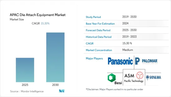
아시아태평양의 다이 어태치 장비 시장은 예측 기간 동안 15.3%의 CAGR을 기록할 것으로 예상됩니다.
주요 하이라이트
5G는 미래 기술 혁신을 위한 통합 연결 플랫폼으로, 훨씬 더 빠른 데이터 및 비디오 전송과 지속적인 보안 클라우드 액세스를 가능하게 하는 5G를 지원하는 소형의 매우 복잡한 스마트폰용 다이본딩 및 패키징 솔루션 개발에 초점을 맞추고 있습니다. 미션에서 지속적인 보안 클라우드 액세스를 가능하게 합니다.
사용자들이 5G 기능을 채택함에 따라 모바일 브로드밴드 활동이 확대되고, 만물인터넷(Internet of Everything)을 향한 인공지능의 활용이 가속화될 것입니다. 마찬가지로 모바일 인터넷, 컴퓨팅, 5G, 차량용 최종사용자를 위한 기판 및 웨이퍼 레벨 패키징 공정은 반도체 산업의 메모리 및 로직 설비 투자 회복을 이끌었습니다.
회사는 반도체와 FPD 용도 확대를 위한 중장기 설비투자 증가 계획을 공유하고 있습니다. 한편, 반도체 조립장비에서는 FOWLP/PLP 및 μLED용 고속/고정밀 본딩 장비의 적극적인 개발이 주목됩니다.
BESI는 FOWLP, TCB, TSV, 초박형 다이, 하이브리드 본딩, 대면적, 웨이퍼 레벨 몰드, 태양광, 3D 리튬이온 배터리 도금 등 새로운 디지털 사회에 대응하는 새로운 조립 기술에 대한 투자 계획을 공유하고 있습니다. 다이 어태치 장비는 싱글칩, 멀티칩, 멀티모듈, 플립칩, TCB, FOWLP, 하이브리드 다이본딩 시스템, 다이소팅 시스템 등 다양한 라인업을 갖추고 있습니다.
그러나 우려스러운 점은 COVID-19의 전 세계적 확산으로 인한 불확실성이 지속되고 있다는 점입니다. COVID-19의 확산으로 인한 아시아태평양의 가동 중단과 생산 중단은 반도체 생산과 소비에 큰 영향을 미쳤습니다. 가동 중단의 영향은 설비 투자에 대한 지출 감소로 이어졌습니다. 이는 2021년까지 회복세가 둔화될 것으로 예상되는 시장 조사에 영향을 미칠 가능성이 높습니다.
아시아태평양의 다이 어태치 장비 시장 동향
CIS는 큰 폭의 성장이 예상
CMOS 이미지 센서는 스마트폰 및 기타 제품에 카메라 기능을 제공해 왔으나, 미세화 수요가 확대됨에 따라 팹에서 제조상의 문제가 발생하고 있습니다.
3G에서 4G로, 현재는 5G로 데이터 성능의 광대역화가 진행되면서 더 높은 품질의 카메라에 대한 수요가 증가하고 있습니다. 이러한 추세는 더 높은 픽셀 수와 해상도의 필요성에 따른 CMOS 이미지 센서의 적층 기술을 촉진해 왔습니다. 이 외에도 생체인식 ID, 3D 센싱, 강화된 인간 시각 애플리케이션 분야가 성장세를 보이고 있습니다.
더 크고 더 좋은 카메라에 대한 고객의 요구로 인해 더 큰 다이 사이즈의 센서가 증가하고 있습니다. 픽셀 스케일링 외에도 CMOS 이미지 센서는 다이 스태킹과 같은 기술 혁신이 진행되고 있습니다. 이 시장의 벤더들은 실리콘 관통 전극(TSV), 하이브리드 본딩, 픽셀 간 본딩 등 다양한 상호연결 기술을 사용하고 있습니다.
예를 들어, 하이브리드 본딩의 경우, 다이와 다이를 구리-구리 상호연결로 연결합니다. 이를 위해 팹에서 두 개의 웨이퍼를 가공하는데, 하나는 로직 웨이퍼이고 다른 하나는 픽셀 어레이 웨이퍼이며, 두 웨이퍼는 유전체-유전체 접합으로 접합된 후 금속-금속 접합으로 접합됩니다.
Xperi의 독자 기술인 하이브리드 접합 DBI 기술은 삼성 휴대폰용 CMOS 이미지 센서 제조에 많이 활용되고 있으며, CMOS 이미지 센서용 이 기술은 상온에서 Cu-Cu 영구 접합, 저온 어닐링(약 300℃), 외압을 가하지 않는 접합 공정(유전체/금속)을 용이하게 합니다. 유전체/금속)을 용이하게 합니다.
이에 앞서 다이렉트 본드 기술은 15년 이상 Xperifor가 주도한 여러 세대의 픽셀 스케일링(후면 조사) BSI와 적층 BSI를 실현하는 데 있어 실현 가능한 역할을 해왔습니다.
점유율을 독식하는 LED
다이 어태치 재료는 중/고/초고출력 LED의 성능과 신뢰성에 중요한 역할을 하며, LED 보급률이 증가함에 따라 다이 어태치 장비에 대한 수요가 증가하고 있습니다. 특정 칩 구조와 용도에 적합한 다이 어태치 재료의 선택은 패키징 공정(처리량 및 수율), 성능(방열 및 광 출력), 신뢰성(루멘 유지), 비용 등 다양한 고려사항에 따라 결정되며, LED의 다이 어태치에는 공융 주석, 은을 함유한 에폭시, 솔더, 실리콘, 솔더, 실리콘, 납땜, 실리콘, 에폭시, 실리콘, 실리콘 등 다양한 재료가 사용됩니다. 솔더, 실리콘, 소결 재료 등이 사용되어 왔습니다.
SFE는 LED 에폭시 다이본더 기계의 인덱싱 시간 0.2초/사이클(가동률 90%), 칩 크기 250*250 표준, 2대의 카메라로 리드프레임 인식을 제공하는 에폭시 접착제 본딩 방식을 제공합니다. 소프트웨어 기능은 자동 마운트 레벨 및 픽업 레벨 티칭 기능을 제공합니다.
또한, 전도성 접착제(주로 은으로 채워진 에폭시)는 LED용 열접착 재료의 최대 클래스(수량 기준)를 구성하고 있습니다. 이들은 기존 백엔드 패키징 장비와 호환되며, 매력적인 비용 대비 성능 균형(일반적으로 2차 리플로우 호환, 최대 50W/mK의 열)을 제공합니다. 베어 실리콘에 부착되기 때문에 GaN on Silicon과 같이 백엔드 금속화가 없는 다이에 가장 선호되는 재료입니다.
또한, LED 시장에는 많은 경쟁업체가 존재하지만, ASM은 이 시장에 진입한 대표적인 기업 중 하나이며, ASM의 LED 에폭시 고속 다이본더 AD830은 LED 시장을 독점하고 있습니다. 고속, 고신뢰성, 고정밀, 다이 배치 정밀도는 +/-1mil, +/-3도, 10mil x 10mil과 같은 소형 칩의 사이클 타임은 180ms이며, 이는 1,8,000UPH에 해당합니다. 사전 설정된 배치 범위에서 본딩된 유닛을 모니터링하는 포스트 본드 검사 시스템이 장착되어 있습니다.
아시아태평양의 다이 어태치 장비 산업 개요
아시아태평양의 다이 어태치 장비 시장은 경쟁이 치열하며, 많은 기업들이 작은 시장 점유율을 가지고 있습니다. 각 업체들은 시장 점유율을 유지하기 위해 기술 혁신을 지속하고 전략적 파트너십을 맺고 있습니다.
2022년 4월 - Electric Revolution Industrialization Centre(DER-IC) North East는 파워 일렉트로닉스, 기계, 드라이브(PEMD) 능력을 향상시키기 위해 공구 및 재료의 선도적인 기술 유통 업체인 Inseto로부터 장비를 수령하였습니다. 영국에서 최초로 도입되는 마이크로 펀치 머신은 AMX P100 소결 프레스이며, 고신뢰성, 고출력 모듈 생산을 가능하게 하는 장비의 일부입니다.
2022년 6월 - West Bond가 새로운 7KF 본더 시리즈를 개발했습니다. 이 유명한 회사는 마이크로 전자 패키징 산업을 위한 와이어 본딩 기계, 다이투어터치 기계, 와이어 인장 검사기, 전단 검사기, 초음파 부품 및 액세서리 제품 라인을 설계 및 제조하고 있습니다. 이 우수한 도구는 RF, 마이크로파, 반도체, 하이브리드, 의료기기 부문에서 볼 수 있는 까다로운 본딩 응용 분야를 처리하기 위해 만들어졌습니다.
기타 혜택
엑셀 형식의 시장 예측(ME) 시트
3개월 애널리스트 지원
목차
제1장 소개
조사 가정과 시장 정의
조사 범위
제2장 조사 방법
제3장 주요 요약
제4장 시장 역학
시장 개요
산업의 매력 - Porter's Five Forces 분석
공급 기업의 교섭력
구매자의 교섭력
신규 참여업체의 위협
대체품의 위협
경쟁 기업 간의 경쟁 관계
산업 밸류체인 분석
COVID-19가 시장에 미치는 영향
제5장 시장 성장 촉진요인
AuSn 공정 다이 어태치 기술 수요 확대
디스크리트 파워 디바이스 수요
제6장 시장 과제
가공·수명중 치수 변화와 기계적 언밸런스
제7장 시장 세분화
본딩 기술
다이 본더
에폭시/접착제(페이스트/필름)
공정
납땜
소결
플립칩 본더
픽 앤 플레이스/리플로우 솔더링
서모컴프레션(TCB)
서모소닉 본딩
하이브리드 본딩
용도
메모리
LED
로직
CMOS 이미지 센서
옵토일렉트로닉스/포토닉스
디스크리트 파워 디바이스
MEMS & 센서
적층 메모리 & RF
국명
대만
중국
일본
한국
동남아시아
제8장 경쟁 구도
기업 개요
Palomar Technologies, Inc.
Shinkawa Ltd
Panasonic Corporation
ASM Pacific Technology Limited
Be Semiconductor Industries NV(Besi)
Shibaura Mechatronics Corporation
ficonTEC Trading Ltd(ficonTEC Service GmbH)
Fasford Technology Co Ltd.
Dongguan Hoson Electronic Technology Ltd
For Technos Co., Ltd.
Shenzhen Xinyichang Technology Co., Ltd.(Hoson)
제9장 벤더의 시장 점유율 분석 - 2021년
제10장 투자 분석
제11장 투자 분석 시장 전망
ksm
영문 목차
영문목차
The APAC Die Attach Equipment Market is expected to register a CAGR of 15.3% during the forecast period.
Key Highlights
A significant focus for the next investment round by market vendors is developing die bonding and packaging solutions for smaller and highly complex 5G compatible smartphones. 5G is a unifying connectivity platform for future innovation, enabling continuous secure cloud access at significantly higher data and video transmission speeds.
User adoption of 5G capabilities expands mobile broadband activities and accelerates artificial intelligence usage for the Internet of Everything. Likewise, the substrate and wafer-level packaging processes for mobile internet, computing, 5G, and automotive end-user applications drove the semiconductor industry to see a recovery in capital investment for memories and logic.
The company has shared plans for a medium-to-long-term increase in capital investment towards expanded semiconductor and FPD applications. Whereas, as per Shibaura, active development of high-speed, high-precision bonding equipment for FOWLP / PLP and μLED is being looked out for in semiconductor assembly equipment.
BESI has shared plans to invest in new assembly technologies such as FOWLP, TCB, TSV, ultra-thin dies, hybrid bonding, large area, wafer level molding, solar, and 3D-lithium-ion battery plating for the new digital society. Its lineup under Die attach equipment includes a single chip, multi-chip, multi-module, flip chip, TCB, FOWLP, hybrid die bonding systems, and die sorting systems.
However, one source of concern is the continuing uncertain outlook due to the impact of the global spread of COVID-19. Lockdowns and production halts across Asia-pacific due to the COVID-19 outbreak had significantly impacted the production and consumption of semiconductors. With the majority of the IDS and foundries located in the region, the impact of shutdowns has led to reduced spending on capital investments. This is likely to impact the market studied, with a slowed recovery expected across 2021.
APAC Die Attach Equipment Market Trends
CIS is expected to witness significant growth
CMOS image sensors have been offering camera functions in smartphones and other products, and as the scaling demand grows, the related manufacturing issues in the fab arise.
The higher-bandwidth data performance progressed from 3G to 4G, and currently, to 5G, the demand for higher quality cameras has grown. This trend has propelled the CMOS image sensor stacking techniques based on the need for higher pixel counts and better resolution. Beyond these trends, the areas of biometric ID, 3D sensing, and enhanced human vision applications have augmented segment growth.
Customer demand for bigger and better cameras results in more sensors with bigger die sizes. Besides pixel scaling, CMOS image sensors are undergoing other innovations like die stacking. Vendors in the market studied are also using different interconnect technologies, such as through-silicon vias (TSVs), hybrid bonding, and pixel-to-pixel for the same.
In hybrid bonding, for instance, the dies are connected using copper-to-copper interconnects. For this, two wafers are processed in a fab. One is the logic wafer, while the other is the pixel array wafer. The two wafers are joined using a dielectric-to-dielectric bond, followed by a metal-to-metal connection.
Hybrid bonding DBI technologies, Xperi'sproprietary technology, are being significantly used by Samsung towards CMOS image sensor fabrication for its phones. This technology for CMOS Image Sensors facilitates room temperature Cu-Cu permanent bonding, low-temperature annealing (around 300°C) & no external pressure bonding process (dielectric/metal).
Prior to this, direct bond technology has thus played an enabling role in the realization of pixel scaling (backside illumination) BSI and stacked BSI with multiple generational variations led by Xperifor over 15 years.
LED to dominate market share
Die attach material represents a key role in the performance and reliability of mid, high, and super-high power LEDs. The demand for die-attach equipment is increasing with an increasing LED penetration rate. The selection of suitable die-attach material for a particular chip structure and application depends on various considerations, which include the packaging process (throughput and yield), performance (thermal dissipation output and light output), reliability (lumen maintenance), and cost. Eutectic gold-tin, silver-filled epoxies, solder, silicones, and sintered materials have all been used for LED die attach.
SFE provides an Epoxy Adhesive bonding method where its LED Epoxy Die Bonder machine features an index time of 0.2 Sec /Cycle (90 Percent Rate of Operation) with a chip size of 250 * 250 standards, providing lead frame recognition through 2 Cameras. Its software function provides auto mount level & pick up level teaching functions.
Further, conductive adhesives (mostly silver-filled epoxies) constitute the largest class of thermal die-attach materials (by unit number) for LEDs. They are compatible with existing back-end packaging equipment and provide an attractive cost/performance balance (typically up to 50 W/mK thermals with secondary reflow compatibility). As they stick to bare silicon, they are the most preferred material for dies without back-end metallization like GaN on silicon.
Further, in the LED market, there are a lot of rival competitors, and ASM is one of the prominent players in this market; its LED Epoxy High speed die bonder AD830 dominates in the LED market. It is fast, reliable, and accurate with die placement accuracy of +/-1 mil and +/-3 degree, cycle time for a small chip like 10mil x 10mil is 180 ms, which is an equivalent UPH of 18,000. It is equipped with a Post bond inspection system that monitors the bonded unit at the pre-set placement range.
APAC Die Attach Equipment Industry Overview
The APAC Die attach equipment market is moderately competitive, with a large number of players having a small market share. The companies keep innovating and entering into strategic partnerships to maintain their market share.
April 2022 - Driving the Electric Revolution Industrialization Centre (DER-IC) North East has received equipment from Inseto, a top technical distributor of tools and materials, to improve its power electronics, machines, and drives (PEMD) capabilities. The first micro-punch machine to be installed in the UK is an AMX P100 sinter press, which is part of the equipment provided and will allow the production of high-reliability, high-power modules.
June 2022 - The new 7KF Bonder Series has been developed by West Bond. This well-known company designs and manufactures a line of wire bonding and die-to-attach machines, wire pull and shear test equipment, ultrasonic components, and accessories for the microelectronics packaging industry. This excellent tool is made to handle the difficult bonding applications found in the RF, microwave, semiconductor, hybrid, and medical device fields.
Additional Benefits:
The market estimate (ME) sheet in Excel format
3 months of analyst support
TABLE OF CONTENTS
1 INTRODUCTION
1.1 Study Assumptions and Market Definition
1.2 Scope of the Study
2 RESEARCH METHODOLOGY
3 EXECUTIVE SUMMARY
4 MARKET DYNAMICS
4.1 Market Overview
4.2 Industry Attractiveness - Porter's Five Forces Analysis
4.2.1 Bargaining Power of Suppliers
4.2.2 Bargaining Power of Buyers
4.2.3 Threat of New Entrants
4.2.4 Threat of Substitutes
4.2.5 Intensity of Competitive Rivalry
4.3 Industry Value Chain Analysis
4.4 Impact of Covid-19 on the market
5 Market Drivers
5.1 Growing Demand of AuSn Eutectic Die-Attach Technology
5.2 Demand of Discrete Power Devices
6 Market Challenges
6.1 Dimensional Changes During Processing and Service Life and Mechanical Unbalance
7 MARKET SEGMENTATION
7.1 By Bonding Technique
7.1.1 Die Bonder
7.1.1.1 Epoxy/Adhesive (paste/film)
7.1.1.2 Eutectic
7.1.1.3 Solder
7.1.1.4 Sintering
7.1.2 Flip Chip Bonder
7.1.2.1 Pick and Place / reflow soldering
7.1.2.2 Thermocompresion (TCB)
7.1.2.3 Thermosonic Bonding
7.1.2.4 Hybrid Bonding
7.2 Application
7.2.1 Memory
7.2.2 LED
7.2.3 Logic
7.2.4 CMOS Image Sensor
7.2.5 Optoelectronics / Photonics
7.2.6 Discrete Power Devices
7.2.7 MEMS & Sensors
7.2.8 Stacked Memory & RF
7.3 Country
7.3.1 Taiwan
7.3.2 China
7.3.3 Japan
7.3.4 Korea
7.3.5 Southeast Asia
8 COMPETITIVE LANDSCAPE
8.1 Company Profiles
8.1.1 Palomar Technologies, Inc.
8.1.2 Shinkawa Ltd
8.1.3 Panasonic Corporation
8.1.4 ASM Pacific Technology Limited
8.1.5 Be Semiconductor Industries NV (Besi)
8.1.6 Shibaura Mechatronics Corporation
8.1.7 ficonTEC Trading Ltd (ficonTEC Service GmbH)