ㅁ Add-on 가능: 고객의 요청에 따라 일정한 범위 내에서 Customization이 가능합니다. 자세한 사항은 문의해 주시기 바랍니다.
ㅁ 보고서에 따라 최신 정보로 업데이트하여 보내드립니다. 배송기일은 문의해 주시기 바랍니다.
한글목차
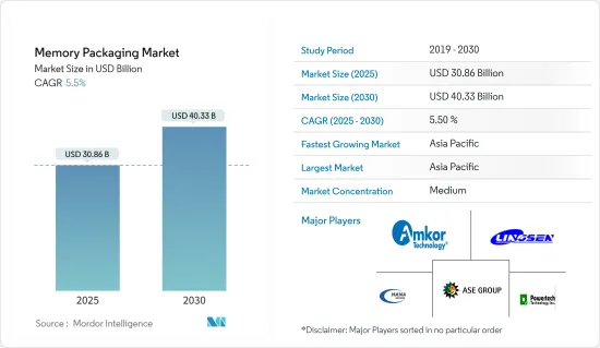
메모리 패키징 시장 규모는 2025년에 308억 6,000만 달러로 추정되고, 예측 기간 2025년부터 2030년까지의 CAGR은 5.5%로 전망되며, 2030년에는 403억 3,000만 달러에 달할 것으로 예측됩니다.
최근 COVID-19의 유행은 아시아태평양, 특히 중국이 조사 대상 시장의 주요 영향요인 중 하나이기 때문에 조사 대상 시장 공급망에 큰 불균형을 가져올 것으로 예상됩니다. 또한 아시아태평양 지방 정부의 대부분은 장기적인 프로그램으로 반도체 산업에 투자하고 있기 때문에 시장 성장을 되찾을 것으로 기대됩니다. 예를 들어, 중국 정부는 국가 IC 투자 기금 2030의 두 번째 단계에 약 230억-300억 달러의 자금을 조달했습니다. 팬데믹으로부터 시장 회복 시간이 불투명하기 때문에 세계의 여러 지역에 대한 경제적 영향은 반도체 시장의 성장에 큰 과제를 제공하고, 첨단 메모리 패키징 시장에 필요한 중요한 원재료의 이용 가능성에 세계적으로 직접 영향을 미칠 것으로 예상됩니다.
주요 하이라이트
메모리 디바이스는 플립 칩, 리드 프레임, 와이어 본드, 스루 실리콘 비아(TSV) 등 광범위한 패키징 기술을 채택하고 있습니다. 칩의 소형화와 고기능화에 따라 외부 회로와의 전기적 접속 수가 증가하고 있습니다.
이것은 패키징 기술의 개발로 이어지고 있습니다. 플립칩, TSV, 웨이퍼 레벨 칩 스케일 패키징(WLCSP)은 광대역화, 고속화, 패키지의 소형화 및 박형화를 충족하는 유망한 기술입니다. 알기 쉬운 프로그램 조정, 낮은 엔지니어링 비용, 쉬운 전환이 와이어 본드 메모리 패키징 플랫폼에 대한 수요를 뒷받침하고 있습니다.
또한 패키징 설계의 변화로 인해 와이어 본드 메모리 패키징 플랫폼은 유연성, 신뢰성 및 저렴한 비용으로 가장 선호되는 상호 연결 플랫폼으로 계속 사용되고 있습니다. 플립칩은 2016년에 DRAM 메모리 패키징으로 진출하기 시작했으며, 고대역폭 요구사항을 뒷받침한 DRAM PC/서버의 채용 증가로 성장이 예상되고 있습니다.
고 대역폭 및 메모리 칩의 낮은 대기 시간은 많은 용도에서 고성능 컴퓨팅에 대한 요구에 박차를 가하고 있으며, 실리콘 관통 전극(TSV)이 고 대역폭 메모리 장치에 채택되었습니다.
메모리 패키징 시장 동향
DRAM이 큰 점유율을 차지할 것으로 예측
이 시장은 모바일과 컴퓨팅(주로 서버) 수요를 목격하고 있습니다. 스마트폰 1대당 DRAM 메모리 용량은 평균 3배 이상 증가하여 2022년에는 약 6GB에 이를 것으로 예상됩니다.
최근 조사 대상 시장의 지배적 선수 중 하나인 Samsung Electronics가 하이엔드 스마트폰을 위한 새로운 메모리 패키징의 양산을 발표했습니다.
모바일 애플리케이션에서 메모리 패키징은 와이어 본드 플랫폼이 주류가 될 것으로 예상됩니다. 하지만 하이엔드 스마트폰용 멀티칩 패키징(ePoP)으로의 전환이 곧 시작될 것으로 보입니다. 엔터프라이즈 아키텍처와 클라우드 컴퓨팅이 향상됨에 따라 컴퓨팅 DRAM 패키징은 예측 기간 동안 큰 성장을 이룰 것으로 예상됩니다.
삼성 HBM2 기술은 8개의 8G비트 DRAM 다이로 구성되며 5,000개의 TSV를 사용하여 적층 연결됩니다. 최근 이 회사는 12개의 DRAM 다이를 적층하고 6만개의 TSV를 사용하여 연결된 새로운 HBM 버전도 발표했습니다.
스마트폰 1대당 DRAM 메모리 용량이 증가하고 있으며, 새로운 장치는 최소 4Gb의 용량을 제공하고 2020년에는 최소 6GB에서 8GB의 용량에 도달할 것으로 예상됩니다. 스마트폰 1대당 NAND 용량이 증가하고 있으며 현재 64GB 이상, 2020년에는 150GB 이상에 이를 것으로 예상되고 있습니다. 서버용으로 1대당 DRAM 용량은 2020년까지 약 1TB로 증가하고, 엔터프라이즈용 SSD의 NAND 용량은 예측 기간 말까지 5TB 이상에 달할 것으로 예측됩니다.
자동차산업이 큰 점유율을 차지
저밀도(저MB) 메모리를 사용하는 자동차 시장에서는 자율주행이나 자동차 인포테인먼트의 동향에 견인되어 DRAM 메모리의 채용이 증가할 가능성이 있습니다. NOR 플래시 메모리 패키징 시장도 터치 디스플레이 드라이버 IC, AMOLED 디스플레이, 산업용 IoT 등 신분야에 대한 용도에 의해 성장이 전망되고 있습니다.
성장 전략의 일환으로 많은 OSAT 기업이 메모리 칩 제조업체와 전략적 제휴를 맺고 있으며, 지역 기업은 세계 기술 제공업체와 제휴하여 시장 도달범위를 확대하고 있습니다.
이 시장에서 사업을 전개하는 제조업체는 생산 시설을 확장하고 있습니다. 예를 들어 SK Hynix Inc.는 한국에서 반도체 패키징 및 검사 시설의 능력을 확대하고 있습니다. 이러한 개발로 기존 기업은 시장 개척 기회를 늘리고 경쟁사는 시장에서 우위를 차지할 수 있을 것으로 보입니다.
패키징 기술에 도입된 기술 혁신은 대형 시스템 온칩(SoC) 솔루션의 기능 밀도 증가와 관련이 있습니다. 그러나 자동차 환경에서의 엄격한 신뢰성 요건과 OSATs 산업의 상황 변화는 예측 기간 동안 시장 성장을 방해할 것으로 예상됩니다.
최근에는 바이오메트릭 센서, CMOS 이미지 센서, 가속도계 등의 MEMS 센서 등 다양한 용도 분야에서 Si 기반 센서 기술의 사용이 증가하고 있습니다. 또한 휴대전화나 PDA 등의 휴대기기에 내장되는 센서 및 디바이스도 늘고 있습니다. 이러한 용도 분야에서는 이 센서 기술을 성공적으로 통합하기 위해 소형, 저비용, 내장성이 필수적입니다.
일반적으로 OEM은 플러그 앤 플레이 모듈 또는 완전한 서브시스템을 선호하지만, 이는 또한 메모리 칩 시장을 돕는 요인이며, 따라서 기술적 용도를 강화하기 위한 메모리 패키징 수요를 이끌고 있습니다.
메모리 패키징 산업 개요
메모리 패키징 시장의 경쟁은 중간 정도입니다. DRAM 메모리의 가격 상승에 따라 메모리 패키징 시장에서 사업을 전개하는 벤더는 3D NAND 개발에 대한 지출을 늘리고 있습니다. SK Hynix Inc.가 발표한 기사에 따르면, 각 회사는 더 이상 3D NAND 수요에 대한 요구가 없어 제조 능력의 확장이 요구되고 있습니다. 또한 많은 기업들이 수요 증가에 대응하기 위해 제조 장비를 확장하고 있습니다. 전반적으로, 예측 기간 동안 시장은 위의 모든 요인들에 대해 고급 경쟁으로 전환할 수 있습니다.
The Memory Packaging Market size is estimated at USD 30.86 billion in 2025, and is expected to reach USD 40.33 billion by 2030, at a CAGR of 5.5% during the forecast period (2025-2030).
The recent COVID-19 outbreak is expected to create significant imbalances in the supply chain of the market studied, as Asia-Pacific, particularly China, is one of the major influencers of the market studied. Also, many of the local governments in the Asia-Pacific have invested in the semiconductor industry in a long run program, hence, expected to regain market growth. For instance, the Chinese government raised around USD 23 to 30 billion funds, to pay for the second phase of its National IC Investment Fund 2030. Owing to the uncertainty in the recovery time of the market from the pandemic, economic impacts on several parts of the world are further expected to provide significant challenges to the growth of the semiconductor market, directly affecting the availability of critical raw materials required for advanced memory packaging market globally.
Key Highlights
Memory devices employed a broad range of the packaging technology that include flip-chip, lead-frame, wire-bond, through-silicon via (TSV). With the decrease in dimensions and increase in the chip functionality, a higher number of the electrical connections have to be made to the external circuit.
This has also led to development in packaging technologies. Flip-chip, TSV, and wafer-level chip-scale Packaging (WLCSP) are promising technologies to satisfy wider bandwidth, faster speed, and smaller/thinner package. Comprehensible program adjustments, low engineering costs, and easy changeovers are fueling the demand for the wire-bond memory packaging platform.
Additionally, due to changes in the package design, the wire-bond memory packaging platform continues to be used as the most preferred interconnection platform because of its flexibility, reliability, and low-cost. Flip-chip began making inroads in the DRAM memory packaging in 2016 and was expected to grow due to its increased adoption in the DRAM PC/server, fueled by high bandwidth requirements.
Spurred on by high bandwidth and memory chips' low latency demands for high-performance computing in numerous applications, through-silicon via (TSV), is being employed in high bandwidth memory devices.
Memory Packaging Market Trends
DRAM is Estimated to Hold Significant Share
The market studied is witnessing demand from mobile and the computing (mainly servers). On average, the DRAM memory capacity per smartphone is anticipated to rise more than threefold to reach around 6GB by 2022.
Recently, Samsung Electronics Co. Ltd, one of the dominant players in the market studied, announced the mass production of the new memory package aimed at high-end smartphones, which may save space by putting DRAM and eMMC together.
For mobile applications, memory packaging is expected to remain on the wire-bond platform mostly. However, it will soon begin moving toward the multi-chip package (ePoP) for high-end smartphones. With the improvement in enterprise architecture and cloud computing, the computing DRAM packaging is anticipated to witness significant growth during the forecast period.
Samsung's HBM2 technology consists of eight 8Gbit DRAM dies, which are stacked and connected using 5,000 TSVs. Recently, the company also launched a new HBM version that stacks 12 DRAM dies, which are connected using 60,000 TSVs and are ideal for data-intensive applications, such as AI and HPC.
DRAM memory capacity per smartphone has risen with new devices offering a minimum of 4 Gb space which is expected to reach a minimum of 6 GB to 8 GB of space by 2020, while NAND capacity per smartphone has increased reaching more than 64 GB now and are expected to become reach over 150 GB by 2020. For servers, DRAM capacity per unit is projected to increase to approximately 1 TB by 2020 and NAND capacity for each SSD for the enterprise market are expected to reach more than 5 TB in capacity by the end of the forecast period
Automotive Industry to Hold Significant Share
The automotive market, which uses the low density (low-MB) memory, might observe an increase in the acceptance of DRAM memory, led by the growing trend of autonomous driving and in-vehicle infotainment. NOR Flash memory packaging market is also expected to grow due to its application in new areas, such as touch display driver ICs, AMOLED display, and industrial IoTs.
As part of the growth strategy, numerous OSAT players are entering into strategic alliances with memory chip manufacturers, and regional players are partnering with global technology providers to increase their reach in the market.
Manufacturers operating in the market are expanding their production facilities. For instance, SK Hynix Inc. is expanding its semiconductor packaging and inspection facility capacity in South Korea. Such developments are expected to help create increased opportunity for the existing players and cut competitors edge in the market studied.
The innovations being introduced in the packaging technology are associated with the growth in functional density of large system-on-chip (SoC) solutions. However, harsh reliability requirements in the automotive environment and changing landscape of the OSATs industry is anticipated to hamper the growth of the market studied over the forecast period.
In recent times, there has been growth in the use of Si-based sensor technology for a variety of applications, including biometric sensors, CMOS image sensors, and MEMS sensors, such as accelerometers. Increasingly, and sensor devices are being integrated into portable devices, like handsets and PDAs. In these applications, small-size, low-cost, and ease-of-integration are essential to incorporate this sensor technology successfully.
Generally, OEMs prefer a plug-and-play module or complete subsystem, which is also a factor that is helping the memory chip market, and in turn, driving the demand for the memory packaging for enhanced technological applications.
Memory Packaging Industry Overview
The memory packaging market is moderately competitive. With the rising prices of DRAM memory, vendors operating in the memory packaging market are increasingly spending on the development of 3D NAND. According to an article published by SK Hynix Inc., companies can no longer keep up with 3D NAND demand and are required to expand their manufacturing capacity. Also, many of the companies are expanding their manufacturing units in order to meet the growing demand. Overall the market might move towards highly competitive during the forecast period due to all the above factors.
Additional Benefits:
The market estimate (ME) sheet in Excel format
3 months of analyst support
TABLE OF CONTENTS
1 INTRODUCTION
1.1 Study Assumptions and Market Definition
1.2 Scope of the Study
2 RESEARCH METHODOLOGY
3 EXECUTIVE SUMMARY
4 MARKET DYNAMICS
4.1 Market Overview
4.2 Industry Attractiveness - Porter's Five Forces Analysis
4.2.1 Bargaining Power of Suppliers
4.2.2 Bargaining Power of Consumers
4.2.3 Threat of New Entrants
4.2.4 Threat of Substitutes
4.2.5 Intensity of Competitive Rivalry
4.3 Industry Value Chain AnalysiS
4.4 Technology RoadmaP
4.5 Assessment of Impact of COVID-19 on the Market
4.6 Market Drivers
4.6.1 Emerging Trend of Autonomous Driving and In-vehicle Infotainment
4.6.2 Increase in Demand for Smartphones
4.6.3 Memory Semiconductor Business Explosion
4.6.4 Continuous Developments in High-bandwidth Memory (HBM) and Redistribution Layer
4.7 Market Challenges
4.7.1 Harsh Reliability Requirements in the Automotive Environment