Thin-Film Electrode Market by Material, Manufacturing Facility, End-Use Industry - Global Forecast to 2030
상품코드:1883932
리서치사:MarketsandMarkets
발행일:2025년 11월
페이지 정보:영문 220 Pages
라이선스 & 가격 (부가세 별도)
ㅁ Add-on 가능: 고객의 요청에 따라 일정한 범위 내에서 Customization이 가능합니다. 자세한 사항은 문의해 주시기 바랍니다.
한글목차
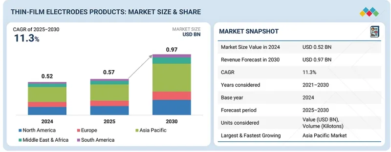
세계의 박막 전극 시장 규모는 2025년 5억 7,000만 달러에서 2030년에는 9억 7,000만 달러에 달할 것으로 예측되며, CAGR로 11.3%의 성장이 전망됩니다.
조사 범위
조사 대상 기간
2021-2030년
기준연도
2024년
예측 기간
2025-2030년
단위
100만/10억 달러, 킬로톤
부문
재료, 제조 기술, 최종 용도 산업, 지역
대상 지역
아시아태평양, 북미, 유럽, 중동 및 아프리카, 남미
박막 전극 시장은 소비자용 및 산업용 전자기기의 소형화, 경량화, 고성능화에 대한 수요 증가에 힘입어 성장하고 있습니다. 스마트폰, 웨어러블 기기, 센서, 마이크로칩 등의 디바이스가 기능성을 높이면서 크기를 계속 축소하고 있는 가운데, 정밀하고 신뢰성이 높으며 전도성이 우수한 박막 전극이 필수적입니다. 물리 기상 성장(PVD)과 화학기상증착(CVD) 기술의 지속적인 발전에는 큰 시장 기회가 존재합니다. 이러한 혁신을 통해 제조업체는 확장성과 재료의 다양성이 향상된 초박형, 균일하고 결함 없는 전극 필름을 생산할 수 있습니다.
"붕소 도핑 다이아몬드는 박막 전극 시장에서 금액 기준으로 가장 빠르게 성장하고 있는 소재 부문입니다. "
붕소 도핑 다이아몬드(BDD) 소재는 뛰어난 화학적 안정성, 넓은 전위차 창, 오염에 대한 내성이 있으며, 까다로운 전기화학 응용 분야에 이상적이며 박막 전극 시장에서 가장 빠르게 성장하고 있는 분야입니다. BDD 전극은 기존의 금속이나 탄소 전극과 달리 부식성이 높은 환경이나 극한의 전위에서도 열화 없이 작동할 수 있으며, 폐수처리, 전기화학 산화, 환경 모니터링 등 첨단 산업에서 사용할 수 있습니다. 붕소 도핑 다이아몬드의 독특한 격자 구조는 높은 전기 전도성과 기계적 경도를 결합하여 전극이 장기간의 작동 주기 동안 성능을 유지할 수 있도록 합니다. 또한 BDD 박막은 낮은 배경 전류와 높은 신호 감도를 보여 바이오센서, 제제 분석, 산업용 정수 시스템을 포함한 분석 및 센싱 용도에서 점점 더 선호되고 있습니다.
"화학기상증착은 박막 전극 시장에서 금액 기준으로 가장 빠르게 성장하고 있는 제조 설비 부문입니다. "
화학기상증착(CVD)은 우수한 기계적, 전기화학적 특성을 가진 고순도, 균일하고 컨포멀한 박막을 생산할 수 있으며, 박막 전극 시장에서 가장 빠르게 성장하고 있는 제조 기술입니다. CVD는 박막의 조성, 두께, 결정구조를 정밀하게 제어할 수 있으며, 특히 붕소도핑다이아몬드(BDD), 탄소전극과 같은 첨단 소재에서 우위를 점하고 있습니다. 이러한 재료는 원자 수준의 균일성과 기판과의 견고한 접착력을 요구하는데, CVD는 기존 기술보다 더 효과적으로 이러한 특성을 구현할 수 있습니다. 그 결과, 이 기술은 폐수 처리, 전기 화학적 산화, 고성능 감지 시스템 등 극도의 화학적 안정성과 긴 작동 수명이 요구되는 응용 분야에서 점점 더 선호되고 있습니다. 또한 최근 플라즈마 강화 CVD 공정과 저온 CVD 공정의 혁신으로 온도에 민감한 기판과 유연한 기판에 박막 증착이 가능해져 웨어러블 센서와 바이오 의료기기에서 CVD의 적용 범위가 확대되고 있습니다.
"의료 및 생명공학 분야는 박막 전극 시장에서 금액 기준으로 가장 빠르게 성장하고 있는 최종 용도 산업 분야입니다. "
의료 및 생명공학 산업은 첨단 바이오센싱, 진단 및 신경전자기기 수요 증가로 인해 박막 전극 시장에서 가장 빠르게 성장하고 있는 최종 용도 분야입니다. 박막 전극은 뛰어난 감도, 유연성, 생체적합성을 갖추고 있으며, 전기화학 바이오센서, 신경 인터페이스, 웨어러블 건강 모니터, 이식형 의료기기 등의 용도에 적합합니다. 미세한 생체 신호와 화학 반응을 정밀하게 감지하는 능력으로 인해 POC(Point-Of-Care) 검사, 혈당 모니터링, 뇌-컴퓨터 인터페이스 연구 등에 적용되고 있습니다. 전 세계 의료 시스템이 개인화된 실시간 진단으로 전환하는 가운데, 신뢰할 수 있는 소형화, 비침습적 비침습적 센싱 기술에 대한 수요는 계속 가속화되고 있습니다. 생체적합성 재료(금, 백금, 붕소 도핑된 다이아몬드 등)와 유연한 박막 제조 기술(고분자 기판에 저온 CVD 및 스퍼터링 등)의 발전으로 전극을 웨어러블/이식형 생체의료 시스템에 통합할 수 있게 되었습니다.
세계의 박막 전극 시장에 대해 조사분석했으며, 주요 촉진요인과 억제요인, 경쟁 구도, 향후 동향 등의 정보를 제공하고 있습니다.
목차
제1장 서론
제2장 조사 방법
제3장 개요
제4장 중요 인사이트
박막 전극 시장에서의 매력적인 기회
박막 전극 시장 : 재료별
박막 전극 시장 : 제조 기술별
박막 전극 시장 : 최종 용도 산업별
박막 전극 시장 : 국가별
제5장 시장 개요
서론
시장 역학
촉진요인
억제요인
기회
과제
박막 전극 시장에서 생성형 AI의 영향
서론
화학 기업이 다양한 사업 분야에서 AI를 도입
박막 전극 시장에서 생성형 AI의 활용
박막 전극 시장에서 생성형 AI의 영향
제6장 업계 동향
서론
고객 비즈니스에 영향을 미치는 동향/혼란
공급망 분석
원재료 조달
제조·가공
유통·물류
최종 용도·이용
2025년 미국 관세의 영향 - 박막 전극 시장
서론
주요 관세율
가격의 영향 분석
다양한 지역에 대한 중요한 영향
최종 용도 산업에 대한 영향
가격결정 분석
평균 판매 가격 동향(2021-2024년) : 지역별
박막 전극의 평균 판매 가격 동향 : 형상별(2021-2024년)
주요 기업이 제공하는 박막 전극의 평균 판매 가격 동향 : 형상별(2021-2024년)
투자와 자금조달 시나리오
에코시스템 분석
기술 분석
주요 기술
보완 기술
특허 분석
조사 방법
특허 취득수(2015-2024년)
특허 공보의 동향
인사이트
특허 법적 지위
관할 분석
주요 출원자
주요 특허 리스트
무역 분석
수출 시나리오(HS 코드 831110)
수입 시나리오(HS 코드 831110)
주요 컨퍼런스와 이벤트(2025-2026년)
관세와 규제 상황
관세(2024년)
규제기관, 정부기관, 기타 조직
박막 전극에 관한 규제
Porter's Five Forces 분석
주요 이해관계자와 구입 기준
거시경제 전망
사례 연구 분석
제7장 박막 전극 시장 : 재료별
서론
금속 기반
붕소 도프 다이아몬드
탄소 기반
기타 재료
폴리머 기반
산화물 기반
제8장 박막 전극 시장 : 제조 기술별
서론
물리 기상 증착
화학기상증착
전기화학 증착/전기도금
기타 제조 기술
스크린 프린팅
포토리소그래피
제9장 박막 전극 시장 : 최종 용도 산업별
서론
의료·바이오테크놀러지
전자·반도체
에너지·전력
화학·석유화학
기타 최종 용도 산업
수처리·폐수 처리
산업
제10장 박막 전극 시장 - 지역
서론
아시아태평양
중국
일본
인도
한국
대만
기타 아시아태평양
북미
미국
캐나다
멕시코
유럽
독일
프랑스
영국
이탈리아
스페인
기타 유럽
남미
브라질
아르헨티나
기타 남미
중동 및 아프리카
사우디아라비아
아랍에미리트
기타 GCC 국가
남아프리카공화국
기타 중동 및 아프리카
제11장 경쟁 구도
서론
주요 참여 기업의 전략/강점(2021년 1월-2025년 8월)
시장 점유율 분석(2024년)
매출 분석(2021-2025년)
브랜드의 비교
BASI RESEARCH PRODUCTS, INC
MICRUX TECHNOLOGIES
MERCK KGAA
FLEX MEDICAL SOLUTIONS LTD
METROHM DROPSENS
기업 평가 매트릭스 : 주요 기업(2024년)
경쟁 시나리오
제12장 기업 개요
주요 기업
BASI RESEARCH PRODUCTS, INC
MICRUX TECHNOLOGIES
MERCK KGAA
FLEX MEDICAL SOLUTIONS LTD
PALMSENS
MSE SUPPLIES LLC
METROHM DROPSENS
제13장 부록
KSA
영문 목차
영문목차
The thin-film electrode market is projected to reach USD 0.97 billion in 2030, at a CAGR of 11.3% from USD 0.57 billion in 2025.
Scope of the Report
Years Considered for the Study
2021-2030
Base Year
2024
Forecast Period
2025-2030
Units Considered
Value (USD Million/Billion), Volume (Kiloton)
Segments
Material, Manufacturing Technology, End-Use Industry, and Region
Regions covered
Asia Pacific, North America, Europe, Middle East & Africa, and South America
The thin-film electrode market is driven by the growing demand for miniaturized, lightweight, and high-performance electronic devices across consumer and industrial applications. As devices such as smartphones, wearables, sensors, and microchips continue to shrink in size while increasing in functionality, the need for precise, reliable, and conductive thin-film electrodes has become essential. A significant market opportunity exists in the ongoing advancements of Physical Vapor Deposition (PVD) and Chemical Vapor Deposition (CVD) technologies. These innovations enable manufacturers to produce ultra-thin, uniform, and defect-free electrode films with improved scalability and material diversity.
"Boron-doped diamond was the fastest-growing material segment of the thin-film electrode market in terms of value."
Boron-doped diamond (BDD) materials are the fastest-growing segment in the thin-film electrode market due to their exceptional chemical stability, wide potential window, and resistance to fouling, which make them ideal for demanding electrochemical applications. Unlike traditional metal or carbon electrodes, BDD electrodes can operate in highly corrosive environments and under extreme potentials without degrading, enabling their use in advanced industries such as wastewater treatment, electrochemical oxidation, and environmental monitoring. The unique diamond lattice structure, doped with boron, imparts both high electrical conductivity and mechanical hardness, allowing these electrodes to maintain their performance over long operational cycles. Additionally, BDD thin films exhibit low background current and high signal sensitivity, which makes them increasingly preferred in analytical and sensing applications, including biosensors, pharmaceutical analysis, and industrial water purification systems.
"Chemical vapor deposition is the fastest-growing manufacturing facility segment of the thin-film electrode market in terms of value."
Chemical vapor deposition (CVD) is the fastest-growing manufacturing technology in the thin-film electrode market due to its ability to produce high-purity, uniform, and conformal thin films with excellent mechanical and electrochemical properties. CVD allows precise control over the film's composition, thickness, and crystal structure, which is particularly advantageous for advanced materials such as boron-doped diamond (BDD) and carbon-based electrodes. These materials require atomic-level uniformity and strong adhesion to the substrate qualities that CVD delivers more effectively than traditional techniques. As a result, the technology is becoming increasingly preferred for applications demanding extreme chemical stability and long operational lifespans, such as wastewater treatment, electrochemical oxidation, and high-performance sensing systems. Furthermore, recent innovations in plasma-enhanced and low-temperature CVD processes have enabled the deposition of thin films on temperature-sensitive and flexible substrates, thereby expanding the application of CVD in wearable sensors and biomedical devices.
"Healthcare & biotechnology is the fastest-growing end-use industry segment of the thin-film electrode market in terms of value."
The healthcare and biotechnology industry is the fastest-growing end-use segment in the thin-film electrode market, driven by the increasing demand for advanced biosensing, diagnostic, and neuroelectronic devices. Thin-film electrodes offer exceptional sensitivity, flexibility, and biocompatibility, making them ideal for applications such as electrochemical biosensors, neural interfaces, wearable health monitors, and implantable medical devices. Their ability to detect minute biological signals and chemical reactions with high accuracy is driving their adoption in point-of-care testing, glucose monitoring, and brain-computer interface research. As healthcare systems worldwide move toward personalized and real-time diagnostics, the need for reliable, miniaturized, and non-invasive sensing technologies continues to accelerate. Advancements in biocompatible materials (like gold, platinum, and boron-doped diamond) and flexible thin-film fabrication techniques (such as low-temperature CVD and sputtering on polymer substrates) have enabled the integration of electrodes into wearable and implantable biomedical systems.
"Asia Pacific is the fastest-growing market for thin-film electrodes."
Asia Pacific is the fastest-growing region in the thin-film electrode market due to its strong industrial base, rapid technological advancements, and expanding electronics and semiconductor manufacturing ecosystem. Countries such as China, Japan, South Korea, and Taiwan are global leaders in electronics production, driving large-scale demand for high-performance thin-film electrodes used in sensors, integrated circuits, and microelectronic devices. The region also benefits from massive investments in R&D and fabrication facilities, particularly in the areas of semiconductors, biosensors, and flexible electronics, which rely heavily on thin-film electrode technologies for precision, efficiency, and miniaturization. Moreover, the growing healthcare and biotechnology sectors in countries such as India, China, and Japan are increasingly adopting thin-film electrodes for medical diagnostics, neural implants, and wearable health monitoring devices, further accelerating market growth.
In-depth interviews were conducted with Chief Executive Officers (CEOs), marketing directors, other innovation and technology directors, and executives from various key organizations operating in the thin-film electrode market, and information was gathered from secondary research to determine and verify the market size of several segments.
By Company Type: Tier 1 - 50%, Tier 2 - 30%, and Tier 3 - 20%
By Designation: Managers - 15%, Directors - 20%, and Others - 65%
By Region: North America - 30%, Europe - 25%, Asia Pacific - 35%, the Middle East & Africa -5%, and South America - 5%
The thin-film electrode market comprises BASi Research Products, Inc. (US), MicruX Technologies (Spain), Merck KGaA (Germany), Flex Medical Solutions Ltd (Scotland), PalmSens (Netherlands), MSE Supplies LLC (US), and Metrohm DropSens (Spain). The study includes in-depth competitive analysis of these key players in the thin-film electrode market, with their company profiles, recent developments, and key market strategies.
Research Coverage
This report segments the thin-film electrode market on the basis of material, manufacturing technology, end-use industry, and region, and provides estimations for the overall value of the market across various regions. A detailed analysis of key industry players has been conducted to provide insights into their business overviews, products & services, key strategies, and expansions associated with the thin-film electrode market.
Key benefits of buying this report
This research report is focused on various levels of analysis - industry analysis (industry trends), market ranking analysis of top players, and company profiles, which together provide an overall view of the competitive landscape; emerging and high-growth segments of the thin-film electrode market; high-growth regions; and market drivers, restraints, opportunities, and challenges.
The report provides insights into the following pointers:
Analysis of drivers (Growing demand for flexible and wearable technology), restraints (Material limitations and degradation concerns), opportunities (Expanding market for flexible and transparent electronic applications), and challenges (Achieving sustained stability and biocompatibility for thin-film electrodes in practical settings), influencing the growth of the thin-film electrode market.
Market Penetration: Comprehensive information on the thin-film electrode offered by top players in the global thin-film electrode market.
Product Development/Innovation: Detailed insights on upcoming technologies, expansions, and partnerships in the thin-film electrode market.
Market Development: Comprehensive information about lucrative emerging markets, the report analyzes the markets for the thin-film electrode market across regions.
Market Capacity: Production capacity of the companies is provided wherever available, with upcoming capacities for the thin-film electrode market.
Competitive Assessment: In-depth assessment of market shares, strategies, products, and manufacturing capabilities of leading players in the thin-film electrode market.
TABLE OF CONTENTS
1 INTRODUCTION
1.1 STUDY OBJECTIVES
1.2 MARKET DEFINITION
1.3 STUDY SCOPE
1.3.1 MARKETS COVERED AND REGIONAL SNAPSHOT
1.3.2 INCLUSIONS & EXCLUSIONS
1.3.3 YEARS CONSIDERED
1.3.4 CURRENCY CONSIDERED
1.3.5 UNITS CONSIDERED
1.4 LIMITATIONS
1.5 STAKEHOLDERS
2 RESEARCH METHODOLOGY
2.1 RESEARCH DATA
2.1.1 SECONDARY DATA
2.1.1.1 Key data from secondary sources
2.1.2 PRIMARY DATA
2.1.2.1 Key data from primary sources
2.1.2.2 Key primary sources
2.1.2.3 Key participants for primary interviews
2.1.2.4 Breakdown of primary interviews
2.1.2.5 Key industry insights
2.2 BASE NUMBER CALCULATION
2.2.1 SUPPLY-SIDE ANALYSIS
2.2.2 DEMAND-SIDE ANALYSIS
2.3 GROWTH FORECAST
2.3.1 SUPPLY SIDE
2.3.2 DEMAND SIDE
2.4 MARKET SIZE ESTIMATION
2.4.1 BOTTOM-UP APPROACH
2.4.2 TOP-DOWN APPROACH
2.5 DATA TRIANGULATION
2.6 RESEARCH ASSUMPTIONS
2.7 GROWTH FORECAST
2.8 RISK ASSESSMENT
2.9 FACTOR ANALYSIS
3 EXECUTIVE SUMMARY
4 PREMIUM INSIGHTS
4.1 ATTRACTIVE OPPORTUNITIES FOR PLAYERS IN THIN-FILM ELECTRODE MARKET
4.2 THIN-FILM ELECTRODE MARKET, BY MATERIAL
4.3 THIN-FILM ELECTRODE MARKET, BY MANUFACTURING TECHNOLOGY
4.4 THIN-FILM ELECTRODE MARKET, BY END-USE INDUSTRY
4.5 THIN-FILM ELECTRODE MARKET, BY COUNTRY
5 MARKET OVERVIEW
5.1 INTRODUCTION
5.2 MARKET DYNAMICS
5.2.1 DRIVERS
5.2.1.1 Growing demand for flexible and wearable technology
5.2.1.2 Miniaturization in sensors and biosensors
5.2.1.3 Growth in renewable energy technologies
5.2.2 RESTRAINTS
5.2.2.1 Elevated production costs and challenges in scaling manufacturing processes
5.2.2.2 Material limitations and degradation concerns
5.2.3 OPPORTUNITIES
5.2.3.1 Expanding market for flexible and transparent electronic applications
5.2.3.2 Potential for cost savings through adoption of carbon-based electrode materials
5.2.4 CHALLENGES
5.2.4.1 Achieving sustained stability and biocompatibility for thin-film electrodes in practical settings
5.3 IMPACT OF GENERATIVE AI ON THIN-FILM ELECTRODE MARKET
5.3.1 INTRODUCTION
5.3.2 CHEMICAL COMPANIES EMBRACING AI ACROSS VARIOUS BUSINESS AREAS
5.3.3 USE OF GENERATIVE AI IN THIN-FILM ELECTRODE MARKET
5.3.4 IMPACT OF GENERATIVE AI ON THIN-FILM ELECTRODE MARKET
6 INDUSTRY TRENDS
6.1 INTRODUCTION
6.2 TRENDS/DISRUPTIONS IMPACTING CUSTOMER BUSINESS
6.3 SUPPLY CHAIN ANALYSIS
6.3.1 RAW MATERIAL SOURCING
6.3.2 MANUFACTURING & PROCESSING
6.3.3 DISTRIBUTION & LOGISTICS
6.3.4 END-USE APPLICATIONS & UTILIZATION
6.4 IMPACT OF 2025 US TARIFFS-THIN-FILM ELECTRODE MARKET
6.4.1 INTRODUCTION
6.4.2 KEY TARIFF RATES
6.4.3 PRICE IMPACT ANALYSIS
6.4.4 KEY IMPACT ON VARIOUS REGIONS
6.4.4.1 US
6.4.4.2 Europe
6.4.4.3 Asia Pacific
6.4.5 END-USE INDUSTRY IMPACT
6.5 PRICING ANALYSIS
6.5.1 AVERAGE SELLING PRICE TREND, BY REGION, 2021-2024
6.5.2 AVERAGE SELLING PRICE TREND OF THIN-FILM ELECTRODES, BY FORM, 2021-2024
6.5.3 AVERAGE SELLING PRICE TREND OF THIN-FILM ELECTRODES OFFERED BY KEY PLAYERS, BY FORM, 2021-2024
6.6 INVESTMENT AND FUNDING SCENARIO
6.7 ECOSYSTEM ANALYSIS
6.8 TECHNOLOGY ANALYSIS
6.8.1 KEY TECHNOLOGIES
6.8.2 COMPLEMENTARY TECHNOLOGIES
6.9 PATENT ANALYSIS
6.9.1 METHODOLOGY
6.9.2 PATENTS GRANTED, 2015-2024
6.9.3 PATENT PUBLICATION TRENDS
6.9.4 INSIGHTS
6.9.5 LEGAL STATUS OF PATENTS
6.9.6 JURISDICTION ANALYSIS
6.9.7 TOP APPLICANTS
6.9.8 LIST OF MAJOR PATENTS
6.10 TRADE ANALYSIS
6.10.1 EXPORT SCENARIO (HS CODE 831110)
6.10.2 IMPORT SCENARIO (HS CODE 831110)
6.11 KEY CONFERENCES AND EVENTS, 2025-2026
6.12 TARIFF AND REGULATORY LANDSCAPE
6.12.1 TARIFF, 2024
6.12.2 REGULATORY BODIES, GOVERNMENT AGENCIES, AND OTHER ORGANIZATIONS
6.12.3 REGULATIONS RELATED TO THIN-FILM ELECTRODES
6.13 PORTER'S FIVE FORCES ANALYSIS
6.13.1 THREAT OF NEW ENTRANTS
6.13.2 THREAT OF SUBSTITUTES
6.13.3 BARGAINING POWER OF SUPPLIERS
6.13.4 BARGAINING POWER OF BUYERS
6.13.5 INTENSITY OF COMPETITIVE RIVALRY
6.14 KEY STAKEHOLDERS AND BUYING CRITERIA
6.14.1 KEY STAKEHOLDERS IN BUYING PROCESS
6.14.2 BUYING CRITERIA
6.15 MACROECONOMIC OUTLOOK
6.15.1 GDP TRENDS AND FORECASTS, BY COUNTRY
6.16 CASE STUDY ANALYSIS
6.16.1 THIN-FILM ELECTRODES FOR ANODIC STRIPPING VOLTAMMETRY
7 THIN-FILM ELECTRODE MARKET, BY MATERIAL
7.1 INTRODUCTION
7.2 METAL BASED
7.2.1 ADVANCING ELECTRICAL CONDUCTIVITY AND INDUSTRIAL MANUFACTURING COMPATIBILITY
7.3 BORON-DOPED DIAMOND
7.3.1 ENABLING HIGH CHEMICAL STABILITY AND LONG-TERM ELECTROCHEMICAL PRECISION
7.4 CARBON BASED
7.4.1 SUPPORTING HIGH SURFACE AREA, FLEXIBILITY, AND EMERGING PRINTED ELECTRONICS APPLICATIONS
7.5 OTHER MATERIALS
7.5.1 POLYMER BASED
7.5.2 OXIDE BASED
8 THIN-FILM ELECTRODE MARKET, BY MANUFACTURING TECHNOLOGY
8.1 INTRODUCTION
8.2 PHYSICAL VAPOR DEPOSITION
8.2.1 HIGH PRECISION AND SCALABILITY FOR SEMICONDUCTOR AND FLEXIBLE ELECTRONICS MANUFACTURING
8.3 CHEMICAL VAPOR DEPOSITION
8.3.1 ENABLING HIGH-QUALITY CARBON-BASED AND SPECIALTY ELECTRODE COATINGS
8.4 ELECTROCHEMICAL DEPOSITION/ELECTROPLATING
8.4.1 COST-EFFECTIVE METALLIZATION FOR BATTERIES, SENSORS, AND PRINTED ELECTRONICS
8.5 OTHER MANUFACTURING TECHNOLOGIES
8.5.1 SCREEN PRINTING
8.5.2 PHOTOLITHOGRAPHY
9 THIN-FILM ELECTRODE MARKET, BY END-USE INDUSTRY
9.1 INTRODUCTION
9.2 HEALTHCARE & BIOTECHNOLOGY
9.2.1 ENABLING ADVANCED MONITORING, DIAGNOSTICS, AND BIO-INTERFACE
9.3 ELECTRONICS & SEMICONDUCTOR
9.3.1 SUPPORTING MINIATURIZATION AND HIGH-PERFORMANCE INTEGRATED ELECTRONICS
9.4 ENERGY & POWER
9.4.1 ACCELERATING GROWTH IN BATTERIES, FUEL CELLS, AND ELECTROCHEMICAL ENERGY SYSTEMS
9.5 CHEMICAL & PETROCHEMICAL
9.5.1 IMPROVING PROCESS MONITORING, CORROSION DETECTION, AND REAL-TIME SENSING
9.6 OTHER END-USE INDUSTRIES
9.6.1 WATER & WASTEWATER TREATMENT
9.6.2 INDUSTRIAL
10 THIN-FILM ELECTRODE MARKET -REGION
10.1 INTRODUCTION
10.2 ASIA PACIFIC
10.2.1 CHINA
10.2.1.1 Huge electronics manufacturing and rapid semiconductor expansion innovation to drive market
10.2.2 JAPAN
10.2.2.1 Electronics leadership and advanced healthcare sector to drive market
10.2.3 INDIA
10.2.3.1 Strong policy support, expanding semiconductor and electronics base, and rising healthcare innovation collectively to drive market
10.2.4 SOUTH KOREA
10.2.4.1 Semiconductor advancement and technological innovations in electronics to drive market
10.2.5 TAIWAN
10.2.5.1 Semiconductor leadership, high-tech manufacturing, and growing applications in healthcare sector to drive market
10.2.6 REST OF ASIA PACIFIC
10.3 NORTH AMERICA
10.3.1 US
10.3.1.1 Rising healthcare investments and rapid semiconductor expansion to drive market
10.3.2 CANADA
10.3.2.1 Growing healthcare, semiconductors, and clean energy to drive market
10.3.3 MEXICO
10.3.3.1 Rapid industrialization, robust semiconductor ecosystem, and growing healthcare and energy infrastructure to drive market
10.4 EUROPE
10.4.1 GERMANY
10.4.1.1 Strong semiconductor, pharmaceutical, and energy sectors to support market
10.4.2 FRANCE
10.4.2.1 Synergistic growth across semiconductors, electronics, and healthcare to strengthen by large-scale investments
10.4.3 UK
10.4.3.1 Focus on healthcare innovation, semiconductor expansion backed by strong R&D funding, and industrial collaborations
10.4.4 ITALY
10.4.4.1 Cutting-edge healthcare demand, electronics innovation, and semiconductor investment to drive market
10.4.5 SPAIN
10.4.5.1 Expanding electronics manufacturing and chemical industry to drive market
10.4.6 REST OF EUROPE
10.5 SOUTH AMERICA
10.5.1 BRAZIL
10.5.1.1 Strong government backing and thriving manufacturing base to drive market
10.5.2 ARGENTINA
10.5.2.1 Rising healthcare investment, renewable energy initiatives, and broader transition toward advanced materials and high-tech manufacturing to drive market
10.5.3 REST OF SOUTH AMERICA
10.6 MIDDLE EAST & AFRICA
10.6.1 SAUDI ARABIA
10.6.1.1 Expanding renewable projects and healthcare industries to drive market
10.6.2 UAE
10.6.2.1 Huge investments in renewable energy and healthcare innovation to drive market
10.6.3 REST OF GCC COUNTRIES
10.6.4 SOUTH AFRICA
10.6.4.1 Expanding renewable energy projects and advanced healthcare applications to drive market
10.6.5 REST OF MIDDLE EAST & AFRICA
11 COMPETITIVE LANDSCAPE
11.1 INTRODUCTION
11.2 KEY PLAYER STRATEGIES/RIGHT TO WIN (JANUARY 2021-AUGUST 2025)