

반도체 산업에서 박막 형성은 반도체 기판에 정밀하고 제어된 재료 박막 층을 형성하는 방법을 제공하는 반도체 제조 공정에서 중요한 역할을 하고 있습니다. 기술 발전, 진화하는 산업 요구 사항 및 새로운 용도를 반영하는 여러 가지 주목할 만한 트렌드가 반도체 박막 형성 시장을 형성하고 있습니다.
첫째, 높은 처리량, 균일성 및 확장성을 제공하는 박막 형성 기술에 대한 수요가 증가하고 있습니다. 반도체 장비가 점점 더 복잡해지고 집적화됨에 따라 제조업체들은 더 큰 기판 크기를 수용하고 전체 표면적에 걸쳐 일관된 박막 특성을 구현할 수 있는 박막 형성 방법을 필요로 하고 있습니다. 이러한 추세는 원자층 증착(ALD) 및 화학 기상 성장(CVD)과 같은 혁신적인 증착 공정의 개발을 촉진하고 있으며, 대량 생산이 가능하면서 필름 두께와 조성을 정밀하게 제어할 수 있습니다.

반도체 박막 형성 시장의 또 다른 추세는 박막 형성용 첨단 재료의 채택이 증가하고 있다는 점입니다. 장비의 성능 요구사항이 지속적으로 증가함에 따라 전도성, 광 투과성, 열 안정성 등의 특성을 조정한 박막에 대한 요구가 증가하고 있습니다. 이러한 추세는 차세대 전자기기의 진화하는 요구 사항을 충족시키기 위해 새로운 재료 탐색에 초점을 맞춘 연구개발 활동을 촉진하고 있습니다.
또한 3차원(3D) 반도체 구조 및 이종 집적 플랫폼 제작을 지원하는 박막 형성 기술에 대한 관심이 높아지고 있으며, 3D IC 및 시스템온칩(SoC) 아키텍처와 같은 기술의 등장으로 비평면 상에 박막을 형성하고 정확한 층간 배열을 달성할 수 있는 박막 형성 방법에 대한 요구가 증가하고 있습니다.에 대한 요구가 증가하고 있습니다.
또한 박막 형성 기술과 실시간 공정 최적화 및 결함 검출을 가능하게 하는 in situ 모니터링 및 제어 기능을 통합하는 것이 추세입니다. 첨단 측정 툴와 피드백 메커니즘을 증착 시스템에 통합함으로써 제조업체는 공정 안정성, 수율 및 반복성을 개선하고 반도체 장비의 생산 비용과 시장 출시 시간을 단축할 수 있습니다.
전체적으로 반도체 박막 형성 시장 동향은 우수한 성능, 기능성 및 신뢰성을 갖춘 첨단 전자제품을 제조할 수 있는 혁신적인 솔루션에 대한 업계의 끊임없는 탐구를 보여줍니다. 반도체 기술이 계속 발전하는 가운데 박막 형성은 반도체 산업의 발전과 혁신을 촉진하는 중요한 실현 기술로 남을 것입니다.
반도체 박막 형성 기술 동향은 고정밀화, 재료의 다양화, 장비의 복잡성, 환경적 지속가능성, 공정의 지능화를 특징으로 합니다. 이러한 추세는 새로운 박막 형성 방법과 재료의 개발을 형성하고 전례 없는 성능과 기능을 갖춘 차세대 전자기기를 향해 반도체 산업을 주도하고 있습니다.
반도체 박막 형성 기술의 환경은 전자기기의 소형화, 성능 향상, 비용 효율성에 대한 끊임없는 추구로 인해 크게 변화하고 있습니다. 이러한 변화는 반도체 산업 수요 변화와 이러한 요구를 충족시키기 위해 고안된 기술 혁신을 반영하는 몇 가지 주요 트렌드를 통해 특징지어질 수 있습니다.
원자층 증착법(ALD)과 같은 기술은 한 번에 한 원자층씩 증착할 수 있으므로 막의 두께와 조성을 매우 정밀하게 제어할 수 있다는 점에서 각광받고 있습니다. 이러한 정밀도는 미세한 오차가 기기의 성능에 큰 영향을 미치는 차세대 반도체 장비 제조에 매우 중요하며, ALD는 복잡한 3차원 구조를 컨포멀하게 증착할 수 있으므로 3차원 집적회로(IC), 첨단 메모리 기술 등 첨단 용도에 필수적입니다.
기존의 실리콘 기반 반도체는 고유전체, 금속 산화물, 그래핀 및 전이금속 디칼코게나이드와 같은 2차원(2D) 재료와 같은 다양한 신소재로 보강되거나 대체되고 있습니다. 이러한 재료는 전기적, 열적, 기계적 특성이 뛰어나 고성능, 저전력 소비 장비의 개발을 가능하게 합니다. 이러한 재료들을 도입하기 위해서는 고유한 특성과 집적화 문제를 해결할 수 있는 증착 기술의 발전이 필요합니다.
세계의 반도체 시장에 대해 조사분석했으며, 성막 기술 상황의 미래 전망을 제공하고 있습니다. 또한 우선해야 할 연구과제, 해결 기다리는 기술적 과제, 예측되는 시장의 이동을 분명히 하고 있습니다.
In the semiconductor industry, thin film deposition plays a crucial role in the manufacturing process of electronic devices, providing a method to deposit thin layers of materials onto semiconductor substrates with precision and control. Several notable trends are shaping the semiconductor thin film deposition markets, reflecting advancements in technology, evolving industry requirements, and emerging applications.
Firstly, there is a growing demand for thin film deposition techniques that offer high throughput, uniformity, and scalability. As semiconductor devices become increasingly complex and integrated, manufacturers require deposition methods that can accommodate larger substrate sizes and deliver consistent film properties across the entire surface area. This trend is driving the development of innovative deposition processes, such as atomic layer deposition (ALD) and chemical vapor deposition (CVD), which offer precise control over film thickness and composition while enabling high-volume production.
Another trend in the semiconductor thin film deposition markets is the increasing adoption of advanced materials for thin film deposition. As device performance requirements continue to escalate, there is a growing need for thin films with tailored properties, such as enhanced electrical conductivity, optical transparency, and thermal stability. This trend is driving research and development efforts focused on exploring new materials to meet the evolving demands of next-generation electronic devices.
Furthermore, there is a rising emphasis on thin film deposition techniques that support the fabrication of three-dimensional (3D) semiconductor structures and heterogeneous integration platforms. With the advent of technologies like 3D ICs and system-on-chip (SoC) architectures, there is a growing need for deposition methods capable of depositing thin films on non-planar surfaces and achieving precise layer-to-layer alignment.
Moreover, there is a trend towards the integration of thin film deposition techniques with insitu monitoring and control capabilities, enabling real-time process optimization and defect detection. By incorporating advanced metrology tools and feedback mechanisms into deposition systems, manufacturers can enhance process stability, yield, and reproducibility, thereby reducing production costs and time-to-market for semiconductor devices.
Overall, the trends in the semiconductor thin film deposition markets underscore the industry's ongoing quest for innovative solutions that enable the fabrication of advanced electronic devices with superior performance, functionality, and reliability. As semiconductor technologies continue to evolve, thin film deposition will remain a critical enabling technology, driving progress and innovation in the semiconductor industry.
The trends in semiconductor thin film deposition technology are characterized by a move towards greater precision, material diversity, device complexity, environmental sustainability, and process intelligence. These trends are shaping the development of new deposition methods and materials, driving the semiconductor industry towards the next generation of electronic devices with unprecedented performance and functionality.
The landscape of semiconductor thin film deposition technology is undergoing significant transformation, driven by the relentless pursuit of miniaturization, enhanced performance, and cost-efficiency in electronic devices. This evolution is marked by several key trends that reflect the changing demands of the semiconductor industry and the technological innovations designed to meet these needs.
A pivotal trend is the shift towards atomic precision in thin film deposition processes. Techniques such as Atomic Layer Deposition (ALD) are gaining prominence for their ability to deposit films one atomic layer at a time, offering unparalleled control over film thickness and composition. This precision is crucial for manufacturing the next generation of semiconductor devices, where even minor deviations can significantly impact device performance. ALD's ability to conformally coat complex 3D structures makes it indispensable for advanced applications, including 3D integrated circuits (ICs) and advanced memory technologies.

Another significant trend is the diversification of materials used in thin film deposition. Traditional silicon-based semiconductors are being augmented or replaced by a variety of new materials, including high-k dielectrics, metal oxides, and two-dimensional (2D) materials like graphene and transition metal dichalcogenides. These materials offer superior electrical, thermal, and mechanical properties, enabling the development of devices with higher performance and lower power consumption. The incorporation of these materials necessitates advancements in deposition technologies that can handle their unique properties and integration challenges.
The push for greater device integration and functionality is driving the adoption of complex multi-layer structures, which require sophisticated deposition techniques capable of delivering high-quality films with strict interlayer interfaces and uniformity. As devices shrink and the number of layers increases, deposition technologies must offer excellent control over interface engineering, stress management, and layer uniformity to ensure device reliability and performance.
Environmental sustainability and energy efficiency are also becoming critical considerations in thin film deposition processes. The semiconductor industry is increasingly focused on reducing the environmental footprint of manufacturing processes, leading to the development of deposition techniques that consume less energy, use fewer hazardous chemicals, and generate less waste. This trend is not only driven by regulatory pressures but also by the industry's recognition of the importance of sustainable practices for long-term viability.
Lastly, the integration of in-situ monitoring and analytics with deposition processes is a growing trend. Advanced sensors and data analytics are being incorporated directly into deposition systems, enabling real-time process control and optimization. This integration enhances process repeatability, improves yield, and reduces the need for post-deposition inspection, thereby lowering manufacturing costs and improving device performance.
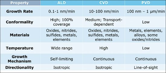
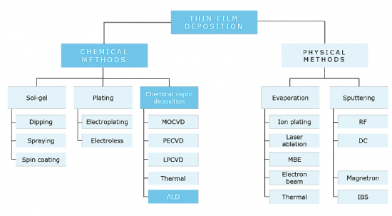
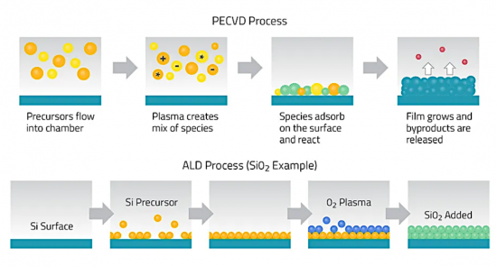
This comprehensive semiconductor deposition report provides an in-depth exploration into the multifaceted domain of deposition technologies pivotal to semiconductor manufacturing. It begins with a foundational overview of thin film deposition, shedding light on critical processes such as physical vapor deposition (PVD), chemical vapor deposition (CVD), atomic layer deposition (ALD), and molecular beam epitaxy (MBE). This section demystifies the principles behind each method, offering a comparative analysis to aid in understanding their unique benefits, limitations, and suitability for various semiconductor applications.
Delving into market dynamics, the report presents a detailed examination of global and regional trends, highlighting market growth, demand patterns, and future projections. It paints a comprehensive picture of the competitive landscape, identifying key players, their market positioning, strategic initiatives, and technological breakthroughs. Furthermore, it discusses the impact of regulatory frameworks and environmental standards on deposition practices, emphasizing the industry's response to sustainability and safety mandates.
Technological advancements occupy a central role in the report, showcasing the latest innovations that enhance film quality, deposition efficiency, and material diversity. It highlights the advent of new materials like 2D materials, high-k dielectrics, and metal oxides that promise to revolutionize semiconductor device performance. The narrative extends to the challenges of integrating these advanced deposition processes into mainstream manufacturing, addressing scalability, quality control, and cost-effectiveness.
The application of deposition technologies in fabricating cutting-edge electronic devices is thoroughly analyzed. This includes their role in developing logic chips, memory devices, power electronics, and their contribution to emerging sectors like 3D integrated circuits (ICs), flexible electronics, and solar cells. The report ventures into the future, speculating on the direction of research and development efforts aimed at overcoming existing technological hurdles, enhancing process capabilities, and discovering environmentally friendly deposition methods.
In its concluding sections, the report provides a forward-looking perspective on the deposition technology landscape, identifying research priorities, technological challenges awaiting resolution, and anticipated market shifts. It features case studies and expert opinions to ground its predictions in real-world examples and authoritative insights, offering readers a wellrounded understanding of the current state and future potential of semiconductor deposition technologies.
By weaving together these diverse strands of information, the report serves as a valuable resource for stakeholders across the semiconductor industry spectrum, from manufacturers and researchers to policymakers and investors, equipping them with the knowledge to navigate the complexities of semiconductor deposition in an era of rapid technological change.
Thin film deposition processes play a critical role in the production of high-density, highperformance microelectronic products. Considerable progress has been achieved in the development of deposition processes -- and in the development of the reactor systems in which they are carried out. This report discusses relevant mechanisms; processing, system, and materials aspects, potential advances, and considerations regarding extendibility to a wafer diameter of 300 mm and beyond.
With the introduction of new thin-film materials to consistently shrinking microelectronic devices and circuits, and as the aperture ratio of an integrated-circuit structure increases, conformal step coverage becomes increasingly difficult to achieve. This report compares some of the issues impacting users of different deposition tools, including:
|
|
|
In addition, as device geometries shrink, semiconductor manufacturing has become increasingly complex and precise, requiring a better understanding of the specific processes involved. These issues are described in the report.
This report discusses the technology trends, products, applications, and suppliers of materials and equipment. It also gives insights to suppliers for future user needs and should assist them in long range planning, new product development and product improvement. A market forecast for Thin Film Deposition Tools is presented including market shares by deposition type between 2012 and 2023.