


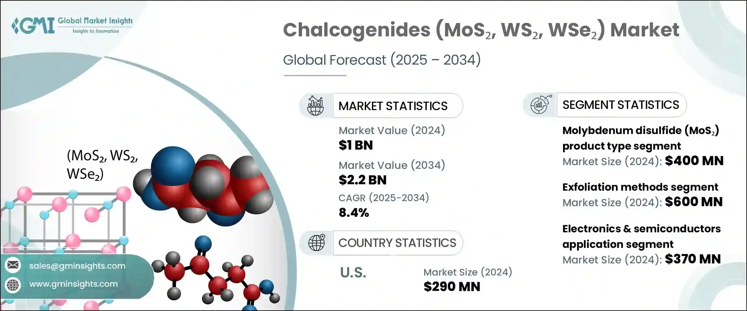
세계의 칼코게나이드(MoS2, WS2, WSe2) 시장은 2024년에는 10억 달러로 평가되었으며 CAGR 8.4%를 나타내 2034년에는 22억 달러에 이를 것으로 추정됩니다.
이러한 꾸준한 성장은 나노기술의 개발과 다수의 산업에 걸친 고성능의 에너지 효율적인 솔루션에 대한 수요 증가로 추진되고 있는 첨단 재료 분야의 폭넓은 기세를 반영하고 있습니다. 실리콘을 기반으로 하는 기술이 물리적·스케일링적인 한계에 직면하는 가운데, 이러한 2차원 재료는 소형화 전자, 플렉서블 디바이스, 고속 트랜지스터 등의 용도에 있어서, 유망한 대체 재료로서 대두해 왔습니다.
미국, 아시아태평양, EU 등 각 지역에서 정부가 지원하는 R&D 이니셔티브는 차세대 재료의 기술 혁신을 추진하기 위해 중요한 재정적·제도적 지원을 제공합니다. 파트너십은 특히 반도체 및 재생에너지 영역에서 강화되고 있으며, 2D 반도체를 유연한 기판에 통합하는 것이 더욱 현실적이 되고 있습니다.
| 시장 범위 | |
|---|---|
| 시작 연도 | 2024년 |
| 예측 연도 | 2025-2034년 |
| 시작 금액 | 10억 달러 |
| 예측 금액 | 22억 달러 |
| CAGR | 8.4% |
제조 기술 중 박리법 부문은 2024년에 6억 달러를 창출했고 2034년까지 연평균 복합 성장률(CAGR) 7.9%를 나타낼 것으로 예측됩니다. 박리법은 여전히 연구 등급의 재료나 프로토타입에 필수적이지만, 화학 기상 성장법(CVD)은 상업 등급 반도체 공정에 적합한 균일하고 고품질의 박막을 얻을 수 있는 능력이 있기 때문에 확장 가능한 생산을 지배하게 되어 있습니다. 폭넓은 기판 적합성, 공업적 생산량으로의 재현성을 가능하게 해, 연구개발로부터 고스루풋 전자기기 제조에의 이행에 최적인 기술로서 자리매김하고 있습니다.
일렉트로믹스 및 반도체 부문은 2024년에 현저한 수익을 올렸습니다. 나노 재료의 독특한 밴드 구조와 반도체 특성은 첨단 전계 효과 트랜지스터, 메모리 디바이스, 박막 논리 회로의 뛰어난 후보가 됩니다. 연구진은 이미 스케일링된 실리콘 기반 디바이스에 필적하거나 이를 상회하는 스위칭 동작과 임계 성능을 보고하고 있으며, 대형 반도체 제조업체가 무어의 법칙 후의 설계 시대에 가까워짐에 따라 이러한 2D 대체 재료의 탐구를 추진하고 있습니다.
미국의 칼코게나이드(MoS2, WS2, WSe2) 시장은 2025-2034년 사이에 현저한 CAGR을 나타낼 것으로 추정되며, 특히 양자기술이나 방위 등급 반도체에의 응용을 위한 연구개발이 견인하고 있습니다. 미국은 다운스트림의 개발과 통합에 선도하고 있으며, 부가가치가 높은 파생품을 국제 시장에 수출하고 있습니다. Material사와 2D Tech사 등 기업들은 국내 연구 노력을 가능하게 하는 데 중요한 역할을 하고 있는 반면, 대규모 방위 계약업체와 전자기기 제조업체는 이러한 고성능 나노 재료 수요를 견인하고 있습니다.
세계의 칼코게나이드(MoS2, WS2, WSe2) 시장에서 사업을 전개하는 유명한 업계 기업은 SixCarbon Technology사, Graphene Laboratories Inc.사, American Elements사, ACS Material LLC사, XFNANO Materials Tech Co. 등이 있습니다. 이러한 기업은 재료 합성과 공급망 개발 모두에 필수적인 존재입니다. 대응하기 위해 생산능력을 확대하고 있습니다. 학술기관이나 국립연구소와의 협력은 특히 양자응용과 플렉서블 전자 등의 최첨단 기술 혁신을 촉진하는 데 도움이 되고 있습니다.
The Global Chalcogenides (MoS2, WS2, WSe2) Market was valued at USD 1 billion in 2024 and is estimated to grow at a CAGR of 8.4% to reach USD 2.2 billion by 2034. This steady growth reflects broader momentum in the advanced materials sector, which is being propelled by developments in nanotechnology and the increasing demand for high-performance, energy-efficient solutions across several verticals. These layered transition metal dichalcogenides have become key enablers in future electronics due to their exceptional electrical, mechanical, and optical behavior. As traditional silicon-based technologies encounter physical and scaling limitations, these 2D materials are emerging as promising alternatives in applications such as miniaturized electronics, flexible devices, and high-speed transistors. The growing interest in compact and power-efficient hardware is particularly relevant in sectors like aerospace, defense, telecommunications, and medical devices.

Government-backed R&D initiatives across regions, including the US, Asia-Pacific, and the EU, are providing crucial financial and institutional support to push next-generation material innovation. This includes establishing national innovation centers, funding pilot manufacturing hubs, and supporting the commercialization of lab-scale research. Public-private partnerships are intensifying, particularly in the semiconductor and renewable energy domains, where the integration of 2D semiconductors into flexible substrates is becoming more feasible. The industry is responding to the growing demand for faster, smaller, and energy-optimized chips, where materials such as MoS2 and WS2 offer considerable performance advantages over legacy materials due to their tunable bandgap and superior carrier mobility.
| Market Scope | |
|---|---|
| Start Year | 2024 |
| Forecast Year | 2025-2034 |
| Start Value | $1 billion |
| Forecast Value | $2.2 billion |
| CAGR | 8.4% |
Among fabrication techniques, the exfoliation methods segment generated USD 0.6 billion in 2024 and is predicted to grow at a CAGR of 7.9% through 2034. While exfoliation remains critical for research-grade materials and prototypes, chemical vapor deposition (CVD) is increasingly dominating scalable production due to its ability to yield uniform and high-quality thin films compatible with commercial-grade semiconductor processes. CVD enables precise layer control, broad substrate compatibility, and reproducibility at industrial volumes, which positions it as the technology of choice for transitioning from R&D to high-throughput electronics manufacturing. Many fabrication labs and pilot facilities have adopted CVD, underlining its pivotal role in bridging lab innovations with commercial-scale applications in nanomaterials.
The electronics & semiconductor segment generated notable revenues in 2024. Their unique band structure and semiconducting properties make them excellent candidates for advanced field-effect transistors, memory devices, and thin-film logic circuits. These materials allow for unprecedented flexibility and ultra-thin architectures, making them highly desirable for next-gen wearable technology, integrated photonics, and soft robotics. Researchers have already reported switching behaviors and threshold performances that match or exceed those of scaled silicon-based devices, which is pushing major semiconductor manufacturers to explore these 2D alternatives as they approach post-Moore's Law design eras.
United States Chalcogenides (MoS2, WS2, and WSe2) Market is estimated to grow at a notable CAGR during 2025-2034, driven by R&D, especially for applications in quantum technology and defense-grade semiconductors. Although bulk materials like MoS2 and WSe2 are largely imported from Asia, the U.S. leads in downstream development and integration, exporting value-added derivatives to international markets. High-tech industries in the U.S. utilize these materials in cutting-edge prototyping, pushing boundaries in optoelectronics, photonics, and next-generation transistor architecture. Companies such as ACS Material and 2D Tech play a critical role in enabling domestic research efforts, while large defense contractors and electronics manufacturers drive demand for these high-performance nanomaterials.
Prominent industry players operating in the Global Chalcogenides (MoS2, WS2, WSe2) market include SixCarbon Technology, Graphene Laboratories Inc., American Elements, ACS Material LLC, and XFNANO Materials Tech Co., Ltd. These companies are integral to both material synthesis and supply chain development. To enhance their market position and expand global reach, leading firms in the chalcogenides industry are leveraging several strategies. They are scaling up production capabilities to meet growing industrial and commercial demand while continuing to invest in high-precision material characterization and customization. Collaborations with academic institutions and national laboratories help foster cutting-edge innovation, particularly in quantum applications and flexible electronics. Key players are also entering strategic partnerships with device manufacturers to co-develop application-specific solutions using 2D materials.