


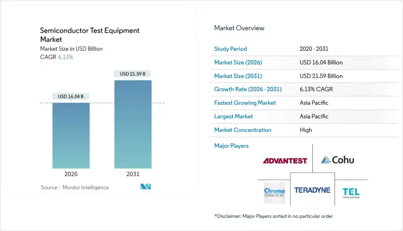
반도체 테스트 장비 시장은 2025년에 151억 1,000만 달러로 평가되었으며, 2026년 160억 4,000만 달러에서 2031년까지 215억 9,000만 달러에 달할 것으로 예측됩니다. 예측 기간(2026-2031년) 동안 CAGR은 6.13%로 전망됩니다.

이러한 수요의 가속화는 AI 프로세서의 복잡성, 자동차의 전동화, 보다 정밀한 검증이 필요한 새로운 패키징 구조의 등장을 반영하고 있습니다. 시스템 레벨 테스트, 광학 검사 및 적응형 분석으로의 빠른 전환은 제조업체가 보다 빠른 고장 식별과 종합적인 장비 효율성 향상을 추구하면서 자본 배분을 재구성하고 있습니다. 아시아태평양은 전 세계 매출의 절반을 차지하고 있으며, 북미와 유럽은 주권 프로그램에 따라 생산능력을 확장하고 있으며, 이로 인해 하이엔드 테스터에 대한 지역 수요가 증가하고 있습니다. 경쟁 우위는 프로브 카드, 분석 소프트웨어 및 용도별 전문 지식을 결합한 공급업체로 이동하고 있습니다. 한편, 자본집약도가 평균 판매가격 상승률을 상회하고 있어 수익률에 대한 압박이 지속되고 있습니다. ATE의 주요 기업과 프로브카드 전문 기업과의 전략적 제휴는 중요한 기계적 인터페이스의 공급망 취약성에 대한 헤지로서 수직적 통합을 강조하고 있습니다.
생성형 AI의 폭발적인 보급은 전례 없는 검증 복잡성을 야기하고, 초고핀 수 디바이스 대응 자동화 테스터의 수요를 증가시키고 있습니다. 웨이퍼 레벨 번인 및 시스템 레벨 제품군 주문 동향은 반도체 테스트 장비 시장이 가속화된 열 스트레스 프로파일 하에서 신뢰성 스크리닝으로 전환하고 있음을 반영합니다. AI 가속기는 거대한 다이 면적과 고급 메모리 스택을 통합하기 때문에 고객들은 설계 단계부터 테스트 지원을 통합한 '설계를 위한 테스트' 후크와 연동되는 적응형 테스터에 투자할 것을 권장하고 있습니다. 어드밴테스트, 2024년 상반기 AI 디바이스 수요에 힘입어 매출과 이익 모두 사상 최대치를 기록. 검증의 고도화가 반도체 제조사의 비용센터가 아닌 공급업체의 수익 창출의 원천이 되었음을 확인시켜주었습니다. 반도체 테스트 장비 업계는 이에 대응하여 커버리지는 그대로 유지하면서 체류 시간을 단축하는 머신러닝 알고리즘을 도입하고 있습니다. 중기적으로는 클라우드 서비스 제공업체와 하이퍼스케일 데이터센터 사업자가 초고속 처리량 시스템 레벨 테스터의 주요 구매자가 될 것입니다.
중앙 집중식 차량 컴퓨팅 아키텍처는 인포테인먼트, 배터리 관리, 레이더 처리를 융합 칩에 통합하고, 기능 안전은 ISO 26262 요구 사항을 충족해야 합니다. 이 전환을 통해 테스트 프로그램의 범위는 파라메트릭 검사에서 도로 이벤트를 모방한 종합적인 시나리오 검증으로 확장됩니다. 키사이트의 인증 툴체인은 설계부터 생산까지 추적성을 지원하며, 컴플라이언스 표준이 반도체 테스트 장비 시장 조달에 어떤 영향을 미치는지 보여줍니다. 자동차용 IC의 신뢰성 검사 시간은 민수용 디바이스에 비해 거의 2배에 달하며, 번인오븐 및 전력 효율을 고려한 핸들러의 수주를 촉진하고 있습니다.
반도체 테스트 장비 업계는 비용 상승과 가격 하락이 수익성에 영향을 미치고 신기술에 대한 투자를 제한하는 도전에 직면해 있습니다. SEMI 보고서에 따르면 2024년 세계 반도체 장비 매출은 1,130억 달러에 달할 것으로 예상되지만, 장비의 복잡성이 가격 결정력을 능가하면서 이익률이 계속 압축되고 있습니다. 고급 패키징 및 칩렛 구조는 고가의 전용 테스트 장비가 필요하며, 고객들은 수익률을 지키기 위해 가격 압박에 직면해 있습니다. KLA Corporation은 반도체 및 웨이퍼 제조 장비 부문의 시장 환경 악화로 인해 2024년 매출은 7% 감소한 98억 달러로, 가격 압박의 영향이 두드러졌다고 보고했습니다. 대용량 애플리케이션의 경우, 고객이 고도의 테스트 기능과 동시에 비용 절감을 요구하기 때문에 추가적인 과제가 발생하고 있습니다. 각 제조사들은 기술적 우위를 유지하기 위해 자동화, 표준화, 연구개발에 집중하고 있습니다.
자동화 테스트 장비는 2025년 반도체 테스트 장비 시장 점유율 37.56%를 유지하며 양산 분야에서 이 카테고리의 확고한 입지를 확인했습니다. 이 부문에는 SoC, 메모리, RF 테스터가 포함되며, 현재는 패턴 커버리지를 가속화하는 AI 지원 진단 기능을 통합하고 있습니다. 어드밴테스트의 T5801은 GDDR7 및 DDR6 디바이스를 검증할 수 있으며, 차세대 메모리 대역폭 요구사항을 충족하기 위해 기존 테스터가 진화하고 있음을 보여줍니다. 핸들러 및 프로브 장치는 병렬 테스트 시 열 균일성과 정밀한 정렬을 보장하고, 핀 수가 많은 장치의 사이트당 비용 절감에 기여합니다.
광학 검사 시스템은 칩렛과 3D 패키지가 기존의 전기 검사로는 감지할 수 없는 시각적 결함을 유발하기 때문에 반도체 테스트 장비 시장 내에서 가장 높은 7.84%의 CAGR을 기록할 것으로 예상됩니다. 적외선 이미징, 표면 하부 균열 감지, AI 지원 결함 분류 기술이 품질 관리 워크플로우를 혁신합니다. 반도체 테스트 장비 시장에서 광학 솔루션 관련 시장 규모는 팹이 전공정 라인과 후공정 라인 모두에서 도입을 진행함에 따라 확대될 것으로 예상됩니다. 전기 데이터와 광학 데이터의 연계를 통해 예측 분석이 가능해져 재작업률 감소와 초기 수율 향상을 실현할 수 있습니다.
아시아태평양은 2025년 반도체 테스트 장비 시장에서 49.62%의 점유율을 차지했으며, 2031년까지 CAGR 7.58%로 확대될 것으로 예상됩니다. 대만에서는 설비투자가 가속화되고 있으며, 킹위안 일렉트로닉스가 AI 칩 테스트 역량 강화에 370억 대만달러(12억 4,000만 달러)를 투자하는 등 지역 내 선도적 입지를 뒷받침하고 있습니다. 중국은 수출 규제를 상쇄하기 위해 국내 툴 개발을 심화시키고 있으며, 동남아시아의 말레이시아와 싱가포르는 후공정 전문성과 실리콘 포토닉스 분야의 틈새시장 강화를 추진하고 있습니다.
북미에서는 CHIPS법 특혜로 인해 520억 달러 이상이 신규 공장에 유입되어 테스트 장비 및 계측기기에 대한 병행 투자를 촉진했습니다. 인텔이 ASML의 고NA EUV 장비를 도입한 것은 3nm 이하 공정 노드에서의 양산 확대를 의미하며, 첨단 ATE 도입의 촉매제가 될 것입니다. 유럽은 1,000억 유로(116억 5,000만 달러)를 투자한 드레스덴 파운드리 합작사를 통해 자율성을 추구하고 있으며, 자동차 고객을 위한 맞춤형 프로브 카드 및 시스템 레벨 랙에 대한 수요가 점차 증가하고 있습니다. 독일에서는 인텔과 Wolfspeed의 시설 건설 계획을 포함하여 더 광범위한 클러스터가 이 지역의 공구 소비를 더욱 다양화시키고 있습니다.
중동 및 아프리카는 아직 발전 초기 단계이지만 정책적으로 반도체 자급자족에 관심을 보이고 있습니다. 걸프협력회의(GCC) 회원국들은 설계 센터와 인재 파이프라인에 자금을 지원하고 있으며, 이는 지역화된 테스트 허브로 발전할 가능성이 있습니다. 수출 규제의 긴장으로 인해 전 세계 공급이 분절되어 각 지역이 중요한 인터페이스 부품을 국내에서 확보하게 되었습니다. 따라서 반도체 테스트 장비 시장은 순수한 비용 최적화보다 공급망 복원력이 더 중요한 다극화 상황에 적응하고 있습니다.
The semiconductor test equipment market was valued at USD 15.11 billion in 2025 and estimated to grow from USD 16.04 billion in 2026 to reach USD 21.59 billion by 2031, at a CAGR of 6.13% during the forecast period (2026-2031).
Demand acceleration reflects the rising complexity of AI processors, automotive electrification, and new packaging architectures that necessitate more precise validation. Rapid migration toward system-level testing, optical inspection, and adaptive analytics reshapes capital allocation as manufacturers pursue faster fault isolation and higher overall equipment effectiveness. The Asia-Pacific region anchors half of global revenue, yet North America and Europe are stepping up capacity under sovereignty programs that are widening regional demand for high-end testers. Competitive advantages shift toward suppliers that combine probe cards, analytics software, and application-specific expertise, while margin pressure persists because capital intensity grows faster than average selling prices. Strategic partnerships between ATE leaders and probe card specialists emphasize vertical integration as a hedge against supply chain fragility in critical mechanical interfaces.
Explosive uptake of generative AI creates unprecedented validation complexity that elevates automated testers equipped for very-high-pin-count devices. Order momentum for wafer-level burn-in and system-level suites reflects the semiconductor test equipment market pivot toward reliability screening under accelerated thermal stress profiles. AI accelerators integrate massive die areas and advanced memory stacks, prompting customers to invest in adaptive testers that synchronize with design-for-test hooks. Advantest reported new highs for revenue and profit in the first half of fiscal 2024 based on AI device demand, confirming that verification intensity is now a profit driver for suppliers rather than a cost center for chipmakers. The semiconductor test equipment industry responds by embedding machine-learning algorithms that cut dwell time without compromising coverage. Over the medium term, cloud service providers and hyperscale data-center operators will remain the dominant purchasers of ultra-high-throughput system-level testers.
Centralized vehicle compute architectures merge infotainment, battery management, and radar processing onto fusion chips whose functional safety must meet ISO 26262 requirements. This transition enlarges the test program scope from parametric checks to holistic scenario validation that mirrors on-road events. Keysight's certified toolchain underpins traceability from design to production, signaling how compliance criteria shape procurement in the semiconductor test equipment market. Reliability screening time for automotive-grade ICs stands nearly 2 times consumer-grade devices, fueling orders for burn-in ovens and power-aware handlers.
The semiconductor test equipment industry faces challenges as rising costs and declining prices impact profitability and limit investments in new technologies. SEMI reported global semiconductor equipment sales reached USD 113 billion in 2024, but margin compression persists as equipment complexity outpaces pricing power. Advanced packaging and chiplet architectures require specialized testing equipment, which comes at a higher cost, and face pricing pressure from customers as they protect their margins. KLA Corporation reported a 7% decline in revenue to USD 9.8 billion in fiscal 2024, driven by weaker market conditions in the semiconductor and wafer fabrication equipment sectors, highlighting the impact of pricing pressures. High-volume applications face added challenges as customers demand cost reductions alongside advanced testing capabilities. Manufacturers are focusing on automation, standardization, and research and development to maintain technological leadership.
Other drivers and restraints analyzed in the detailed report include:
For complete list of drivers and restraints, kindly check the Table Of Contents.
Automated test equipment retained 37.56% of the semiconductor test equipment market share in 2025, underscoring the category's entrenched position in volume production. The segment includes SoC, memory, and RF testers that now integrate AI-enabled diagnostics to accelerate pattern coverage. Advantest's T5801 validates GDDR7 and DDR6 devices, demonstrating that conventional testers are evolving to address the next-generation memory bandwidth requirements. Handler and probe equipment ensure thermal uniformity and precise alignment during parallel testing, lowering cost-per-site for high-pin-count devices.
Optical inspection systems are projected to record an 7.84% CAGR, the fastest within the semiconductor test equipment market, as chiplet and 3D packages introduce visual defects that traditional electrical checks miss. Infrared imaging, subsurface crack detection, and AI-assisted defect classification reshape quality control workflows. The semiconductor test equipment market size associated with optical solutions is expected to increase as fabs deploy them in both front-end and back-end lines. Partnerships between electrical and optical data will enable predictive analytics that cut rework rates and uplift first-pass yield.
The Semiconductor Test Equipment Market Report is Segmented by Product Type (Automated Test Equipment, Burn-In Systems, and More), Application (Wafer Sort/Probe, Final Test, System-Level Test, Reliability/Burn-in), End-Use Industry (Consumer Electronics, Automotive and Mobility, and More), and Geography (North America, South America, Europe, Asia-Pacific, and More). The Market Forecasts are Provided in Terms of Value (USD).
Asia-Pacific dominated the semiconductor test equipment market with a 49.62% share in 2025 and is on track for a 7.58% CAGR to 2031. Taiwan accelerates capex, with King Yuan Electronics allocating NTD 37 billion (USD 1.24 billion) to boost AI chip testing capacity, underscoring regional leadership. China deepens domestic tool development to offset export controls, while Southeast Asia's Malaysia and Singapore reinforce back-end specialization and silicon-photonics niches.
North America benefits from CHIPS Act incentives that funnel over USD 52 billion into new fabs, instigating parallel investment in testers and metrology. Intel's receipt of ASML's high-NA EUV tool signals volume ramp at sub-3 nm nodes, a catalyst for advanced ATE adoption. Europe pursues sovereignty through the EUR 10 billion (USD 11.65 billion) Dresden foundry joint venture, creating incremental demand for probe cards and system-level racks tailored to automotive clients. Germany's broader cluster, including planned Intel and Wolfspeed facilities, further diversifies regional tool consumption.
The Middle East and Africa remain nascent but show policy-driven interest in semiconductor self-sufficiency. Gulf Cooperation Council states finance design centers and talent pipelines that may evolve into localized testing hubs. Export-control tensions fragment global supply, pushing regions to secure critical interface components internally. The semiconductor test equipment market, therefore, adapts to a multipolar landscape in which supply-chain resiliency trumps pure cost optimization.