프로브 핀 시장 : 포고 유형별, 스탬핑 유형별, 스프링 컨택트별, 비스프링 컨택트별, 반도체 시험별, 주파수 범위별, 지역별 - 세계 예측(-2032년)
Probe Pin Market by Pogo Type, Stamping Type, Spring Contact, Non-Spring Contact, Semiconductor Testing (Wafer-level Testing, and Package-level Testing), Frequency Range, and Region - Global Forecast to 2032
상품코드:1928860
리서치사:MarketsandMarkets
발행일:2025년 12월
페이지 정보:영문 249 Pages
라이선스 & 가격 (부가세 별도)
ㅁ Add-on 가능: 고객의 요청에 따라 일정한 범위 내에서 Customization이 가능합니다. 자세한 사항은 문의해 주시기 바랍니다.
한글목차
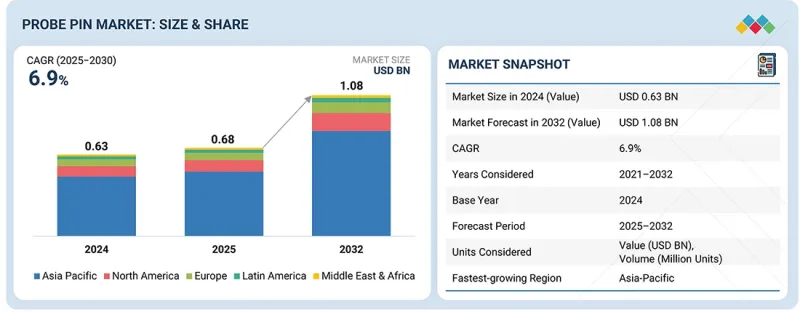
세계의 프로브 핀 시장 규모는 2025년 6억 8,000만 달러에서 2032년까지 10억 8,000만 달러에 달할 것으로 추정되고, 예측 기간 동안 CAGR로 6.9%의 성장이 전망됩니다.
조사 범위
조사 대상 기간
2020-2032년
기준 연도
2024년
예측 기간
2025-2032년
단위
10억 달러
부문
포고 유형, 스탬핑 유형, 주파수 범위, 반도체 시험, 지역
대상 지역
북미, 유럽, 아시아태평양, 기타 지역
세계 프로브 핀 시장은 반도체의 복잡성 증가, 첨단 패키징 채택, 소형화 및 고성능 전자기기로의 전환으로 인해 꾸준한 성장세를 보이고 있습니다. 반도체 팹과 OSAT는 테스트 정확도 향상, 신호 무결성 강화, 웨이퍼 레벨, 패키지 레벨, PCB 테스트의 미세 피치 및 고주파 요구사항에 대응하기 위해 고정밀 프로브 기술에 대한 투자를 확대하고 있습니다. AI, HPC, 5G, EV 파워 디바이스, 칩렛 기반 아키텍처의 확대로 인해 더 높은 전류, 더 엄격한 공차, 더 낮은 접촉 저항에 대응할 수 있는 프로브에 대한 수요가 더욱 증가하고 있습니다. 마이크로 스프링 구조, 정밀 가공, 도금 기술, 자동 제조의 발전으로 프로브의 수명이 연장되고, 불합격품이 감소하며, 대량 생산 환경에서의 일관성이 향상되었습니다.
"자동차 및 EV 부문은 프로브 핀 시장의 최종 사용 산업 부문에서 가장 빠른 성장을 기록할 것으로 예상됩니다."
자동차 및 전기자동차(EV) 산업은 예측 기간 동안 프로브 핀 시장에서 가장 빠른 성장을 기록할 것으로 예상됩니다. 이는 차량의 급속한 전동화, 차량 1대당 반도체 함량 증가, 그리고 첨단 운전자 보조 시스템(ADAS), 배터리관리 시스템(BMS), 파워 일렉트로닉스로의 전환에 기인합니다. 현대의 EV는 고전류, 고온 환경에서의 작동이 요구되며, 안전성이 매우 중요한 반도체 부품에 크게 의존하고 있습니다. 이러한 부품은 웨이퍼 레벨, 패키지 레벨, PCB 레벨에서 엄격한 테스트가 요구됩니다. 이에 따라 자동차의 엄격한 인증 기준 하에서 안정적인 전기적 접촉을 유지할 수 있는 내구성, 저저항, 미세한 피치의 프로브 핀에 대한 수요가 크게 증가하고 있습니다. 자동차 제조업체와 1차 협력업체들이 온보드 컴퓨팅, 인포테인먼트, 커넥티비티 모듈, SiC/GaN 파워 디바이스에 대한 투자를 가속화하고 있는 가운데, 프로브 핀 제조업체들은 복잡한 자동차 테스트 환경에 대응하기 위해 고신뢰성 제품군을 확장하고 있습니다. 아시아태평양, 유럽, 북미에서 전기자동차 보급이 확대됨에 따라 자동차 부문은 프로브 핀 소비량에서 다른 최종 용도 그룹을 능가할 것으로 예상됩니다.
"웨이퍼 레벨 테스트는 프로브 핀 시장의 반도체 테스트 애플리케이션 부문에서 가장 큰 점유율을 차지할 것으로 예상됩니다."
웨이퍼 레벨 테스트는 첨단 반도체 제조로의 급속한 전환과 집적회로의 복잡성 증가로 인해 프로브 핀 시장에서 가장 큰 비중을 차지할 것으로 예상됩니다. 디바이스의 미세화, 3D 적층, 팬아웃 WLP, 칩렛 기반 아키텍처 등 패키징 기술이 발전함에 따라 웨이퍼 프로브에는 정확한 전기적 접촉을 보장하기 위해 초미세 피치, 고주파, 고전류에 대응하는 프로브 핀이 요구되고 있습니다. 반도체 팹은 디바이스가 패키징 공정에 들어가기 전에 웨이퍼 레벨 테스트에 의존하여 조기 결함 감지, 수율 향상, 비용 최적화를 달성하고 있습니다. 이에 따라 로직, 메모리, RF, 아날로그, 자동차, 파워 디바이스 검증에 있어 미세 피치의 고밀도 프로브가 중요해졌습니다. AI 가속기, HPC 프로세서, EV용 전력 반도체, 5G 통신칩의 채용 확대에 따라 주요 파운드리 및 OSAT의 웨이퍼 레벨 테스트 부하가 크게 증가하고 있습니다. 그 결과, 각 프로브 핀 제조업체는 대규모 웨이퍼 프로빙의 엄격한 성능 요구 사항을 충족시키기 위해 마이크로 스프링 설계, 도금 내구성 및 정밀 가공 기술을 향상시키기 위해 노력하고 있습니다.
"북미가 2025년 시장 점유율 2위를 차지할 것으로 예상됩니다."
북미는 반도체 제조업체, 첨단 패키징 기술 개발 기업, 전자 설계 기업의 강력한 입지를 바탕으로 세계 프로브 핀 시장에서 두 번째 점유율을 차지할 것으로 예상됩니다. 이 지역은 정교한 웨이퍼 레벨/패키지 레벨의 테스트가 요구되는 AI 프로세서, 자동차 전자제품, 클라우드 인프라 칩, 통신용 반도체 등의 주요 기업으로부터 혜택을 받고 있습니다. 데이터센터, EV 플랫폼, 항공우주 전자기기, 국방용 반도체 소자에 대한 투자가 고정밀 프로브 핀의 채택을 더욱 가속화하고 있습니다.
세계의 프로브 핀 시장에 대해 조사 분석했으며, 주요 촉진요인 및 저해요인, 제품 개발 및 혁신, 경쟁 구도에 대한 정보를 전해드립니다.
The global probe pin market is estimated to reach USD 1.08 billion by 2032, up from USD 0.68 billion in 2025, at a CAGR of 6.9% during the forecast period.
Scope of the Report
Years Considered for the Study
2020-2032
Base Year
2024
Forecast Period
2025-2032
Units Considered
Value (USD Billion)
Segments
By Pogo Type, Stamping Type, Frequency Range, Semiconductor Testing and Region
Regions covered
North America, Europe, APAC, RoW
The global probe pin market is experiencing steady growth, driven by the increasing complexity of semiconductors, the adoption of advanced packaging, and the shift toward compact, high-performance electronics. Semiconductor fabs and OSATs are increasingly investing in high-precision probe technologies to improve test accuracy, enhance signal integrity, and support fine-pitch and high-frequency requirements across wafer-level, package-level, and PCB testing. The expansion of AI, HPC, 5G, EV power devices, and chiplet-based architectures further increases demand for probes capable of handling higher currents, tighter tolerances, and lower contact resistance. Advancements in micro-spring structures, precision machining, plating technologies, and automated manufacturing are extending probe life, reducing test failures, and improving consistency in high-volume production environments.
"Automotive & EV to register the fastest growth in the end-user industry segment in the probe pin market."
The automotive and electric vehicle (EV) industry is projected to register the fastest growth in the probe pin market during the forecast period, driven by the rapid electrification of vehicles, increasing semiconductor content per car, and the shift toward advanced driver-assistance systems (ADAS), battery management systems (BMS), and power electronics. Modern EVs rely heavily on high-current, high-temperature, and safety-critical semiconductor components that require rigorous wafer-level, package-level, and PCB-level testing. This is significantly boosting demand for durable, low-resistance, and fine-pitch probe pins capable of maintaining stable electrical contact under stringent automotive qualification standards. As automakers and Tier-1 suppliers accelerate investments in on-board computing, infotainment, connectivity modules, and SiC/GaN power devices, probe pin manufacturers are expanding their high-reliability product lines to support complex automotive testing environments. With the rising adoption of EVs across Asia Pacific, Europe, and North America, the automotive segment is expected to outpace all other end-user groups in probe pin consumption.
"Wafer-level testing to account for the largest share in the semiconductor testing application segment in the probe pin market."
Wafer-level testing is expected to account for the largest share of the probe pin market, driven by the rapid transition toward advanced semiconductor manufacturing and the increasing complexity of integrated circuits. As device geometries shrink and packaging technologies evolve, such as 3D stacking, fan-out WLP, and chiplet-based architectures, wafer probe requirements demand ultra-fine-pitch, high-frequency, and high-current probe pins to ensure accurate electrical contact. Semiconductor fabs depend on wafer-level testing for early defect identification, yield improvement, and cost optimization before devices proceed to packaging. This makes fine-pitch and high-density probes critical for validating logic, memory, RF, analog, automotive, and power devices. With the growing adoption of AI accelerators, HPC processors, EV power semiconductors, and 5G communication chips, the wafer-level testing load has increased substantially across leading foundries and OSATs. As a result, probe pin manufacturers are advancing micro-spring designs, plating durability, and precision machining to meet the demanding performance requirements of high-volume wafer probing.
"North America is expected to account for the second-largest market share in 2025."
North America is projected to hold the second-largest share of the global probe pin market, supported by its strong presence of semiconductor manufacturers, advanced packaging innovators, and electronics design houses. The region benefits from major players involved in AI processors, automotive electronics, cloud infrastructure chips, and telecommunications semiconductors, all of which require sophisticated wafer-level and package-level testing. Investments in data centers, EV platforms, aerospace electronics, and defense-grade semiconductor devices further accelerate the adoption of high-precision probe pins. Moreover, the region's strong ecosystem of ATE companies, research institutions, and advanced manufacturing facilities supports continuous innovation in high-frequency and fine-pitch probing technologies. With growing emphasis on domestic semiconductor production, North America is expected to maintain a robust and influential position in the probe pin market.
The break-up of the profile of primary participants in the probe pin market-
By Company Type: Tier 1 - 40%, Tier 2 - 30%, Tier 3 - 30%
By Region Type: Asia Pacific - 45%, Europe - 25%, North America- 20%, Latin America-5%, Rest of the World - 5%
Note: Other designations include sales, marketing, and product managers.
The three tiers of the companies are based on their total revenues as of 2024: Tier 1: >USD 1 billion, Tier 2: USD 500 million-1 billion, and Tier 3: USD 500 million
The major players in the probe pin market with a significant global presence include FEINMETALL (Germany), INGUN (Germany), CCP Contact Probes Co., Ltd. (Taiwan), Seiken Co., Ltd. (Japan), LEENO Industrial Inc. (South Korea), and others.
Research Coverage
The report segments the probe pin market and forecasts its size by contact type, manufacturing method, frequency range, application, end user industry, and region. It also provides a comprehensive review of drivers, restraints, opportunities, and challenges influencing market growth. The report covers qualitative aspects in addition to quantitative aspects of the market.
Reasons to buy the report:
The report will help the market leaders/new entrants in this market with information on the closest approximate revenues for the overall probe pin market and related segments. This report will help stakeholders understand the competitive landscape and gain more insights to strengthen their position in the market and plan suitable go-to-market strategies. The report also helps stakeholders understand the pulse of the market and provides them with information on key market drivers, restraints, opportunities, and challenges.
The report provides insights into the following pointers:
Analysis of key drivers (Growing need for advanced packaging and wafer-level chip-scale packaging, rising SiC & GaN power semiconductor testing, and expansion of OSAT test capacity), restraints (ultra-fine pitch manufacturing limitations, high cost of advanced materials, probe wear, and short life in power testing), opportunities (rapid expansion of automotive electronics and electric vehicle power devices, growth in MEMS, sensor & IoT testing, and development of advanced material coatings and hybrid probe designs), and challenges (low-cost competition from Asian suppliers, and high customization needs and lack of standardization)
Product Development/Innovation: Detailed insights on upcoming technologies, research & development activities, and new product launches in the probe pin market.
Market Development: Comprehensive information about lucrative markets - the report analyses the probe pin market across varied regions.
Market Diversification: Exhaustive information about new products, untapped geographies, recent developments, and investments in the probe pin market.
Competitive Assessment: In-depth assessment of market shares, growth strategies, and product offerings of leading players, including FEINMETALL (Germany), INGUN (Germany), CCP Contact Probes Co., Ltd. (Taiwan), Seiken Co., Ltd. (Japan), and LEENO Industrial Inc. (South Korea).
TABLE OF CONTENTS
1 INTRODUCTION
1.1 STUDY OBJECTIVES
1.2 MARKET DEFINITION
1.3 STUDY SCOPE
1.3.1 MARKETS COVERED AND REGIONAL SCOPE
1.3.2 INCLUSIONS AND EXCLUSIONS
1.3.3 YEARS CONSIDERED
1.4 CURRENCY CONSIDERED
1.5 UNIT CONSIDERED
1.6 STAKEHOLDERS
2 EXECUTIVE SUMMARY
2.1 MARKET HIGHLIGHTS AND KEY INSIGHTS
2.2 KEY MARKET PARTICIPANTS: MAPPING OF STRATEGIC DEVELOPMENTS
2.3 DISRUPTIVE TRENDS IN PROBE PIN MARKET
2.4 HIGH-GROWTH SEGMENTS
2.5 REGIONAL SNAPSHOT: MARKET SIZE, GROWTH RATE, AND FORECAST
3 PREMIUM INSIGHTS
3.1 ATTRACTIVE OPPORTUNITIES FOR PLAYERS IN PROBE PIN MARKET
3.2 PROBE PIN MARKET, BY CONTACT TYPE
3.3 PROBE PIN MARKET, BY MANUFACTURING METHOD
3.4 PROBE PIN MARKET, BY APPLICATION
3.5 PROBE PIN MARKET, BY END-USE INDUSTRY
3.6 ASIA PACIFIC PROBE PIN MARKET, BY END-USE INDUSTRY AND COUNTRY
4 MARKET OVERVIEW
4.1 INTRODUCTION
4.2 MARKET DYNAMICS
4.2.1 DRIVERS
4.2.1.1 Increasing adoption of advanced semiconductor packaging
4.2.1.2 Growing use of SiC and GaN power devices
4.2.1.3 Ongoing expansion of OSAT providers
4.2.1.4 Rapid growth of AI processors, high-performance computing chips, and high-speed ICs
4.2.2 RESTRAINTS
4.2.2.1 Complex manufacturing of ultrafine-pitch probe pins
4.2.2.2 High cost of advanced materials
4.2.2.3 Probe wear and short life in power testing
4.2.3 OPPORTUNITIES
4.2.3.1 Rise of automotive electronics and safety systems
4.2.3.2 Rapid expansion of MEMS devices, sensors, and IoT solutions
4.2.3.3 Development of advanced material coatings and hybrid probe designs
4.2.4 CHALLENGES
4.2.4.1 Intense price competition from low-cost suppliers
4.2.4.2 High customization requirements and limited standardization
4.3 UNMET NEEDS AND WHITE SPACES
4.3.1 UNMET NEEDS
4.3.2 WHITE SPACES
4.4 INTERCONNECTED MARKETS AND CROSS-SECTOR OPPORTUNITIES
4.4.1 INTERCONNECTED MARKETS
4.4.2 CROSS-SECTOR OPPORTUNITIES
4.5 STRATEGIC MOVES BY TIER-1/2/3 PLAYERS
5 INDUSTRY TRENDS
5.1 INTRODUCTION
5.2 PORTER'S FIVE FORCES ANALYSIS
5.2.1 THREAT OF NEW ENTRANTS
5.2.2 THREAT OF SUBSTITUTES
5.2.3 BARGAINING POWER OF SUPPLIERS
5.2.4 BARGAINING POWER OF BUYERS
5.2.5 INTENSITY OF COMPETITIVE RIVALRY
5.3 MACROECONOMIC INDICATORS
5.3.1 INTRODUCTION
5.3.2 GDP TRENDS AND FORECAST
5.3.3 TRENDS IN SEMICONDUCTOR INDUSTRY
5.4 VALUE CHAIN ANALYSIS
5.5 ECOSYSTEM ANALYSIS
5.6 PRICING ANALYSIS
5.6.1 AVERAGE SELLING PRICE OF PROBE PINS OFFERED BY KEY PLAYERS, 2025
5.6.2 AVERAGE SELLING PRICE TREND, BY CONTACT TYPE, 2021-2025
5.6.3 AVERAGE SELLING PRICE TREND, BY REGION, 2021-2025
5.7 TRADE ANALYSIS
5.7.1 IMPORT SCENARIO (HS CODE 9031)
5.7.2 EXPORT SCENARIO (HS CODE 9031)
5.8 KEY CONFERENCES AND EVENTS, 2026-2027
5.9 TRENDS/DISRUPTIONS IMPACTING CUSTOMER BUSINESS