본 서비스는 반도체 첨단 패키징 분야의 특허 활동 관련 최신 데이터(신규 특허 출원 건수, 신규 특허 취득 건수, 특허 만료 및 포기 건수, 특허 양도 건수, 특허 소송 및 이의 제기 현황 등)를 제공합니다.
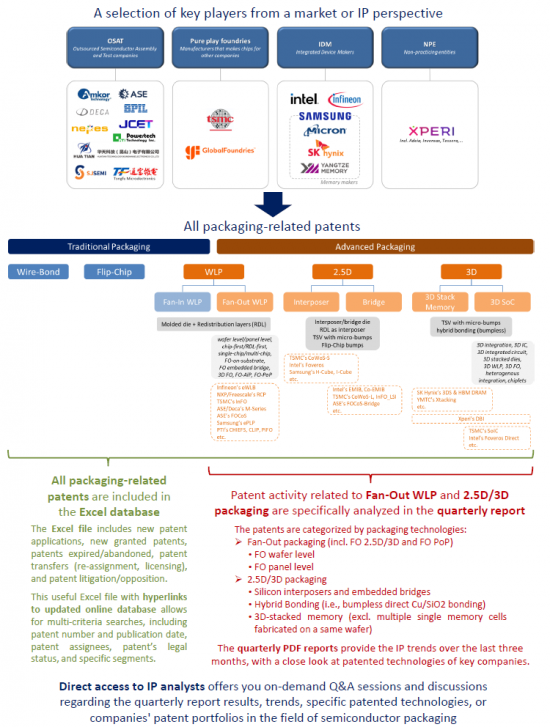
반도체 업계는 폼팩터의 소형화와 제품 성능 향상을 위해 하나의 패키지에 더 많은 연산 능력과 메모리를 집적하려는 수요가 증가하고 있습니다. 그러나 노드의 발전이 한계에 도달함에 따라 무어의 법칙을 달성하는 것은 점점 더 어려워지고 있습니다. 그 결과 칩 소형화 공정이 느려지고 있으며, 2.5D 및 3D 적층 및 팬아웃 웨이퍼 레벨 패키징과 같은 첨단 패키징 기술이 반도체 산업의 요구를 충족시키는 중요한 솔루션으로 부상하고 있습니다. 이러한 새로운 접근 방식은 성숙한 노드와 고급 노드를 결합하여 여러 다이를 단일 패키지에 통합할 수 있게 함으로써 지배적인 플립칩(FC) 및 와이어본드(WB) 기술을 보완하고 있습니다. 이러한 첨단 패키징 기술 로드맵은 고밀도 팬아웃(HD FO) 재배선 레이어(RDL), 고밀도 입출력 상호연결(I/O) 및 실리콘 인터포저, 임베디드 브리지, 하이브리드 본딩, 칩렛 접근 방식과 같은 고급 상호연결 기술에 대한 수요로 인해 공급망 경쟁은 더욱 치열해지고 있습니다. 2.5/3D 패키징 시장이 가장 큰 성장 잠재력을 가지고 있으며, 그 중에서도 3D SoC 기술은 칩렛 3D 집적화를 위한 하이브리드 본딩의 보급으로 가장 큰 성장세를 보이고 있습니다. 팬아웃형 WLP 업계에서는 실리콘 인터포저에 비해 비용 효율적인 솔루션으로 등장한 초고밀도 팬아웃(UHD FO)이 가장 높은 성장세를 보이고 있습니다. 반도체 패키징은 주로 ASE/SPIL, Amkor, JCET와 같은 OSAT에 의해 이루어지고 있으며, 이들은 이 분야에서 중요한 역할을 계속하고 있습니다. 그러나 실리콘 인터포저, 임베디드 브리지, 하이브리드 접합과 같은 혁신적인 2.5D/3D 패키징 솔루션을 개발하는 것은 TSMC, 삼성, 인텔입니다. 첨단 백엔드 솔루션을 제공하고 프론트엔드 역량을 활용함으로써 이들 기업은 이 분야의 미래 기술 및 지적재산권(IP) 발전에 영향을 미칠 수 있는 태세를 갖추고 있습니다.
이러한 상황에서 주요 기업의 특허 활동과 지적재산권(IP) 전략을 모니터링하는 것은 매우 중요합니다. 이러한 지식은 경쟁사의 R&D 로드맵과 전략을 이해하고, 위험을 평가하고, 비즈니스 기회를 포착하는 데 도움이 될 수 있습니다. 이 서비스는 TSMC, Intel, Samsung, Amkor, ASE, SPIL, JCET, Deca, Nepes, Powertech(PTI), SJSemi, Tongfu(TFME), Huatian, Infineon, Micron, SK Hynix, YMTC, GlobalFoundries, Xperi/Adeia 등 주요 기업의 IP 활동을 정기적으로 파악할 수 있습니다.

이 서비스는 분기별로 업데이트되는 엑셀 데이터베이스를 활용하여 분기별 분석 보고서와 애널리스트와의 직접 대화의 이점을 모두 누릴 수 있습니다.

이 서비스를 이용하면 경쟁사의 현재 특허 활동, 지적재산권 동향, 인수 및 라이선스를 포함한 특허 이전, 특허 소송, 기술 개발 및 연구개발 전략을 파악할 수 있습니다. 또한, 사업 분야에 대한 신규 진입을 조기에 감지할 수 있습니다.
최근 특허 출원 동향을 기록해두면 해당 분야의 최신 기술 혁신을 추적할 수 있습니다. 출원된 발명에 대한 세부 정보를 얻고 기술 개발을 추적할 수 있습니다. 새로운 기술 솔루션에서 영감을 받아 R&D 활동을 향상시킬 수 있습니다.
독점적 권리가 부여되기 전에 제출된 특허 출원에 대한 정보를 입수하여 비즈니스에 악영향을 미칠 수 있는 지적재산권 등록을 방지하기 위해 단기간에 대응할 수 있습니다.
새로 발행된 특허를 모니터링하여 자사 제품 및 공정이 특허의 대상이 아닌지 확인하고, 타인의 유효한 지적재산권을 침해하지 않고 안전하게 제조, 판매, 사용할 수 있도록 영업의 자유도를 주기적으로 평가할 수 있습니다.
만료된 특허와 포기된 특허를 모두 추적하여 개발에 안전하게 사용할 수 있는 퍼블릭 도메인 발명을 식별할 수 있습니다.
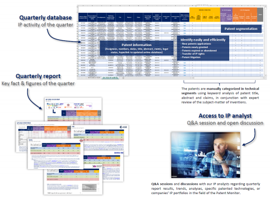
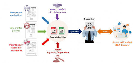
매 분기마다 지난 3개월간의 지식재산권 동향을 주요 지식재산권 기업 및 주요 특허기술에 대한 정보를 제공합니다. 주요 특허 출원인과 그 발명품, 특허, 유망한 특허, 새롭게 만료되거나 포기된 주요 특허를 소개합니다.
전화나 이메일을 통해 애널리스트와 직접 대화하고 질의응답과 공개 토론을 통해 특정 특허 기술이나 기업의 지적재산권 포트폴리오에 대한 구체적인 정보를 얻을 수 있습니다(연간 100시간).

Get up-to-date data on Advanced Semiconductor Packaging patent activity: New patent applications, patents newly granted, expired or abandoned patents, latest patent transfers, patent litigations and oppositions.
In the semiconductor industry, there is a growing demand for integrating more compute and memory within a single package in order to achieve smaller form factors and improve product performance. However, Moore's Law becomes increasingly difficult to achieve as node advancement reaches its limits. As a result, the process of chip miniaturization has been slowing down. Advanced packaging techniques, such as 2.5D & 3D stacking, and fan-out wafer level packaging, have emerged as crucial solutions to meet the needs of the semiconductor industry. These new approaches allow for the integration of multiple dies into a single package, with the possibility of combining mature and advanced nodes, and they have supplemented the dominant flip-chip (FC) and wire-bond (WB) technologies. The roadmap for these advanced packaging technologies is challenging and the supply chain is becoming increasingly competitive, with the demand for high-density fan-out (HD FO) redistribution layers (RDLs), high-density input/output interconnections (I/O), and advanced interconnect technologies such as silicon interposer, embedded bridge, hybrid bonding, and chiplets approach. The market for 2.5/3D packaging shows the most potential for growth, with 3D SoC technology growing the most driven by the increasing popularity of hybrid bonding for chiplets 3D integration. In the fan-out WLP industry, the segment experiencing the highest growth is the ultra-high density fan-out (UHD FO), which has emerged as a more cost-effective solution compared to silicon interposers. Semiconductor packaging was primarily performed by OSATs such as ASE/SPIL, Amkor, JCET, etc. and they continue to play an important role in this field. However, it is TSMC, Samsung and Intel that have been developing innovative 2.5D/3D packaging solutions such as silicon interposer, embedded bridge, and hybrid bonding. By offering advanced back-end solutions and using their front-end capabilities, these companies poised to influence future technology and intellectual property (IP) developments in this area.
In this context, it is crucial to monitor patent activity and intellectual property (IP) strategies of key players. Such knowledge can assist in understanding your competitors' R&D roadmap and strategies, evaluate the risks, and detect business opportunities. The Advanced Packaging Patent Monitor gives periodic insights on the IP activity of a selection of key companies: TSMC, Intel, Samsung, Amkor, ASE, SPIL, JCET, Deca, Nepes, Powertech (PTI), SJSemi, Tongfu (TFME), Huatian, Infineon, Micron, SK Hynix, YMTC, GlobalFoundries, and Xperi/Adeia.
The Advanced Packaging patent monitoring service allows you to take advantage of a quarterly-updated Excel database and benefit from both quarterly analysis reports and direct interaction with our analysts.
With the help of the patent monitoring service, you will be aware of your competitors' current patenting activities, their IP dynamics, patent transfers including acquisitions and licenses, patent litigation, technology development and R&D strategies. You will also be able to early detect new entrants in your business area.
By keeping note of any recent patent filings, you can track the newest innovations in the field. You will get details on claimed inventions and you can follow technology developments. New technical solutions could inspire and improve your R&D activity.
You will obtain information on patent applications filed even before exclusive rights have been granted and you can react in time to prevent registration of IP rights that may be harmful to your business.
Monitoring newly-issued patents allows you to regularly assess your freedom-to-operate, ensuring your products or processes are not covered by patents, and thus that they can be manufactured, sold or used safely without infringing valid IP rights owned by others.
By tracking both expired patents and abandoned patents, you will be able to identify inventions entering the public domain that you can use safely for your development.
On a quarterly basis, the report will provide the IP trends over the three last months, with a close look to key IP players and key patented technologies. Main patent applicants and their inventions, blocking patents, promising patents and key patents newly expired or abandoned will be highlighted.
Take advantage of direct interaction with our analysts by phone call and/or email and get specific input for specific patented technologies and company IP portfolios through Q&A session and open discussion (100h per year).